


16 AMD Geode™ GX Processor/CS5535 Companion Device GeodeROM Porting Guide
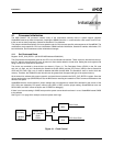
Initialization
32430C
4.1.2 Calculating Processor Speed
Entry Conditions:
Stack and No-Stack versions required.
8254 timer available (port 61).
Procedure:
• Utilize the Real Time Stamp Counter (RTSC).
• Disable the L1 cache.
• Set up a channel of the 8254 Timer chip to count for a predetermined amount of time.
• Read the CPU RTSC and save the initial count value.
• Poll counter and wait for it to roll over.
• Read the CPU RTSC and save as the final count.
• Subtract the initial value of the RTSC from the final value.
• EDX:EAX now contains the number of clock ticks in the predetermined amount of time.
To get the value in MHz, divide the number of clocks by the time represented in microseconds (i.e., 5 ms = 5000).
4.1.2.1 CPU Identification
The CPUID check should be done as soon as possible. Use the CPUID instruction.
Check the Major and Minor Revision fields located in the GLCP_CHIP_REVID register (MSR Address 4C000017h[7:0]) for
the silicon revision.
4.1.3 Memory Controller Initialization
Registers:
MC_CF07_DATA (MSR Address 2000018h)
MC_CF8F_DATA (MSR Address 2000019h)
MC_CFCLK_DBUG (MSR Address 200001Dh)
The memory controller in the GX processor supports SDRAM and DDR memory. The memory controller and the RAM are
programmed via settings read from the SPD. The SPD is required for detection of PC66, PC100, PC133 and DDR RAM.
In the case of a closed system, where the RAM is soldered to the motherboard and there is no SPD, memory settings can
be stored in CMOS for initialization.
The SDRAM clock is set up prior to reset by the clock initialization.
• Address, bank, registered/unbuffered, and other values read from the SPD.
• Size memory in DIMM socket(s).
• Program Memory Controller.
• Set default refresh to an appropriate value.