


ASUS P5LD2 4-27
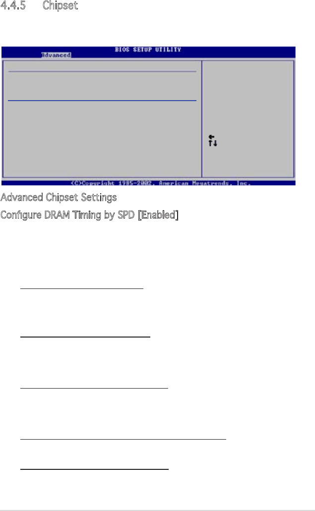
Advanced Chipset Settings
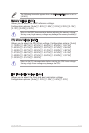
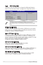
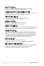
Congure DRAM Timing by SPD [Enabled]
When this item is enabled, the DRAM timing parameters are set according
to the DRAM SPD (Serial Presence Detect). When disabled, you can
manually set the DRAM timing parameters through the DRAM sub-items.
The following sub-items appear when this item is Disabled.
Conguration options: [Disabled] [Enabled]
DRAM CAS# Latency [5 Clocks]
Controls the latency between the SDRAM read command and the time
the data actually becomes available.
Conguration options: [6 Clock] [5 Clocks] [4 Clocks] [3 Clocks]
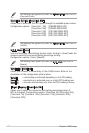
DRAM RAS# Precharge [4 Clocks]
Controls the idle clocks after issuing a precharge command to the DDR
SDRAM. Conguration options: [2 Clocks] [3 Clocks] [4 Clocks]
[5 Clocks] [6 Clocks]
DRAM RAS# to CAS# Delay [4 Clocks]
Controls the latency between the DDR SDRAM active command and
the read/write command. Conguration options: [2 Clocks] [3 Clocks]
[4 Clocks] [5 Clocks] [6 Clocks]
DRAM RAS# Activate to Precharge Delay [15 Clocks]
Conguration options: [4 Clocks] [5 Clocks] ~ [18 Clocks]
DRAM Write Recovery Time [4 Clocks]
Conguration options: [2 Clocks] [3 Clocks] [4 Clocks] [5 Clocks]
[6 Clocks]
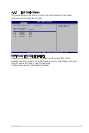
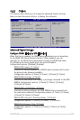
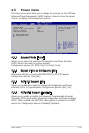
4.4.5 Chipset
The Chipset menu allows you to change the advanced chipset settings.
Select an item then press <Enter> to display the sub-menu.
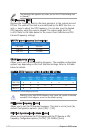
Select Screen
Select Item
+- Change Option
F1 General Help
F10 Save and Exit
ESC Exit
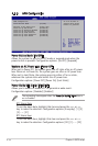
Advanced Chipset Settings
Congure DRAM Timing by SPD [Enabled]
Hyper Path 3 [Auto]
Booting Graphic Adapter Priori [PCI Express/PCI]
PEG Buffer Length [Auto]
Link Latency [Auto]
PEG Root Control [Auto]
PEG Link Mode [Auto]
Slot Power [Auto]
High Priority Port Select [Disabled]
Enable or disable
DRAM timing.