


10
4173ES–USB–09/07
AT89C5132
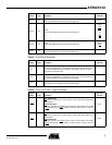
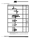
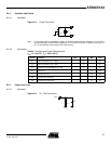
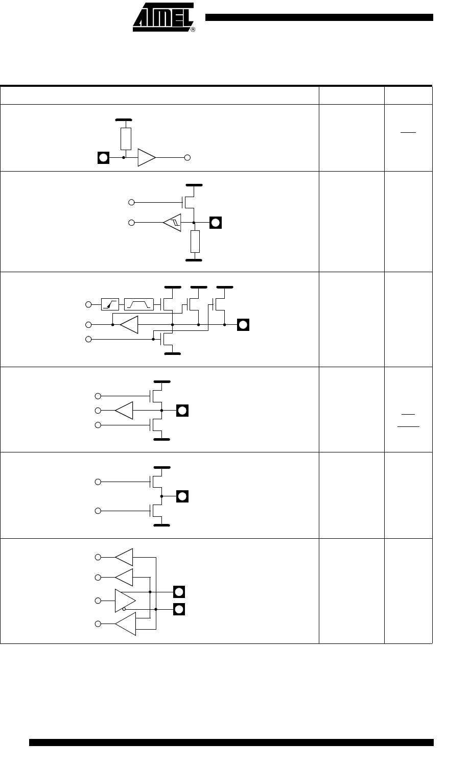
4.2 Internal Pin Structure
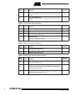
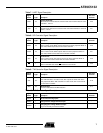
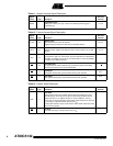
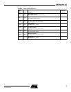
Table 15. Detailed Internal Pin Structure
Notes: 1. For information on resistors value, input/output levels, and drive capability, refer to the
Section “DC Characteristics”, page 183.
2. When the Two Wire controller is enabled, P
1
, P
2
, and P
3
transistors are disabled allowing
pseudo open-drain structure.
3. In Port 2, P
1
transistor is continuously driven when outputting a high level bit address (A15:8).
Circuit
(1)
Type Pins
Input TST
Input/Output RST
Input/Output
P1
(2)
P2
(3)
P3
P4
P53:0
Input/Output
P0
MCMD
MDAT
ISP
PSEN
Output
ALE
SCLK
DCLK
DOUT
DSEL
MCLK
Input/Output
D+
D-
R
TST
VDD
R
RST
VSS
P
VDD
Watchdog Output
P
3
VSS
N
P
1
VDD VDD
2 osc
Latch Output
periods
P
2
VDD
VSS
N
P
VDD
VSS
N
P
VDD
D+
D-