


32
4173ES–USB–09/07
AT89C5132
6.3.8 Flash Memory
6.3.8.1 Definition of Symbols
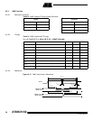
Table 19. Flash Memory Timing Symbol Definitions
6.3.8.2 Timings
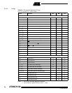
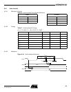
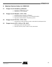
Table 20. Flash Memory AC Timing
V
DD
= 2.7 to 3.3V, T
A
= -40° to +85°C
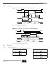
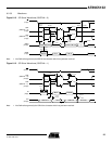
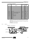
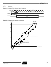
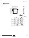
6.3.8.3 Waveforms
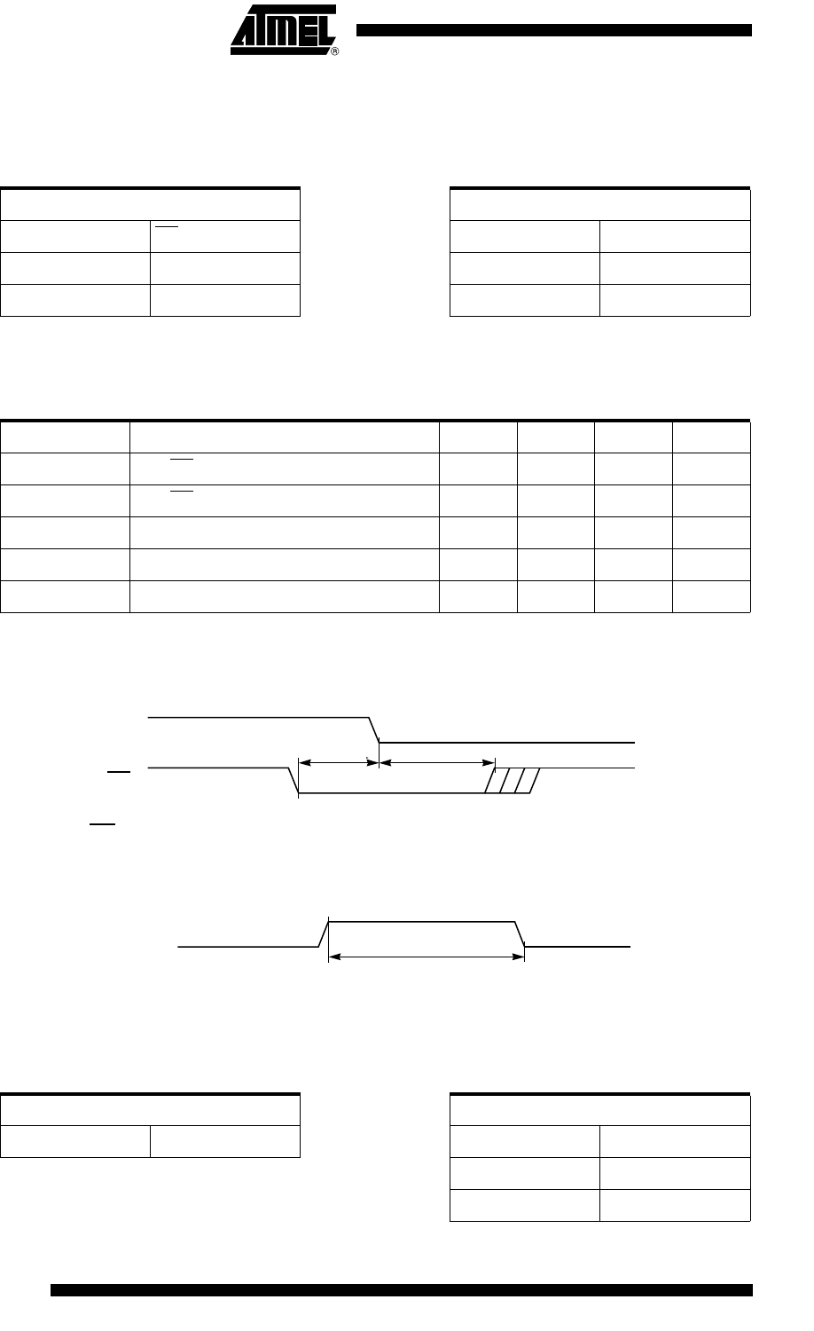
Figure 6-21. Flash Memory – ISP Waveforms
Note: 1. ISP must be driven through a pull-down resistor (see Section “In-system Programming”,
page 18).
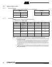
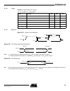
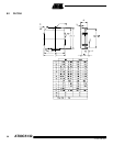
Figure 6-22. Flash Memory – Internal Busy Waveforms
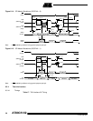
6.3.9 External Clock Drive and Logic Level References
6.3.9.1 Definition of Symbols
Table 21. External Clock Timing Symbol Definitions
Signals Conditions
SISP
L Low
RRST VValid
B FBUSY flag X No Longer Valid
Symbol Parameter Min Typ Max Unit
T
SVRL
Input ISP Valid to RST Edge 50 ns
T
RLSX
Input ISP Hold after RST Edge 50 ns
T
BHBL
FLASH Internal Busy (Programming) Time 10 ms
N
FCY
Number of Flash Write Cycles 100K Cycle
T
FDR
Flash Data Retention Time 10 Year
RST
T
SVRL
ISP
(1)
T
RLSX
FBUSY bit
T
BHBL
Signals Conditions
C Clock H High
L Low
X No Longer Valid