


11
4173ES–USB–09/07
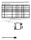
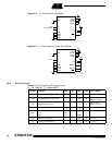
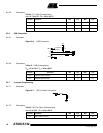
AT89C5132
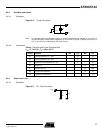
5. Address Spaces
The AT8xC5132 derivatives implement four different address spaces:
• Program/Code Memory
• Boot Memory
• Data Memory
• Special Function Registers (SFRs)
5.0.1 Code Memory
The AT89C5132 implements 64K Bytes of on-chip program/code memory in Flash technology.
The Flash memory increases ROM functionality by enabling in-circuit electrical erasure and pro-
gramming. Thanks to the internal charge pump, the high voltage needed for programming or
erasing Flash cells is generated on-chip using the standard V
DD voltage. Thus, the AT89C5132
can be programmed using only one voltage and allows in application software programming
commonly known as IAP. Hardware programming mode is also available using specific pro
-
gramming tools.
5.0.2 Boot Memory
The AT89C5132 implements 4K Bytes of on-chip boot memory provided in Flash technology.
This boot memory is delivered programmed with a standard bootloader software allowing in sys
-
tem programming commonly known as ISP. It also contains some Application Programming
Interfaces routines commonly known as API allowing user to develop his own bootloader.
5.0.3 Data Memory
The AT89C5132 derivatives implement 2304 bytes of on-chip data RAM. This memory is divided
in two separate areas:
• 256 bytes of on-chip RAM memory (standard C51 memory).
• 2048 bytes of on-chip expanded RAM memory (ERAM accessible via MOVX instructions).