


39
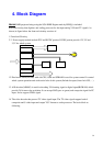
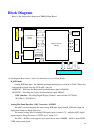
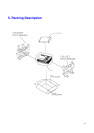
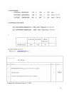
Block Diagram
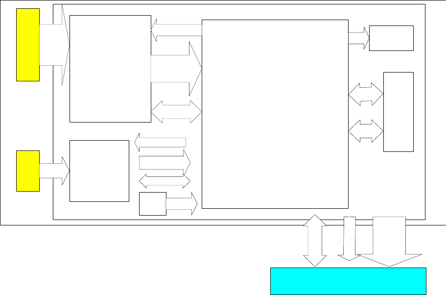
Below is the simple block diagram of PB6100 Main Board .
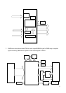
As the diagram shown above , here is the function of every discrete blocks .
- D_SUB input
Analog RGB data input , the standard maximum analog input resolution is SXGA .There also
some interface signals from the VGA cable , they are
ADHSYNC – Providing the Horizontal Synchronization signal to AD9883.
ADVSYNC - Providing the Vertical Synchronization signal AD9883.
DDC interface – Providing Digital Display Channel , which include VCC(Pin9) ,
SCL(Pin15) , SDA(Pin12) .
- Analog Flat Panel Interface (ADC Converter) , AD9883
The ADC converter digitizes the input analog RGB data signal from D_SUB and output the
digital data streams to Image Processor .
The normal voltage level of analog RGB input signals is about 0.7V , while the ADC digital
signal output to Image Processor is LVTTL level , about 3.3V.
The ADC , AD9883 could supports up to pixel rate at about 140MHZ , which is about SXGA
75HZ analog input signal .
D_SUB
S-Video
RCA
Analg Flat Panel
Interface
AD9883
Image Processor
PW166
Flash
EEPROM
RGB 888
Signals
RGB888 signals
A
d
d
r
e
s
s
Data
I2C
I2C
Control Signals
I
2
C
Control Signals
Clock
signal
YUV 422
I2C
Control Signals