


12
256-KBPS LINE DRIVER (V.35, RS-530, OR X.21)
NOTE
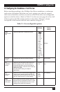
In multipoint applications, do not use the 0-msec option for the
RTS–CTS delay.
2.2.2 M
ODULATION
T
IMING
This circuit supplies the transmit clock to the encoder. Three clock sources are
available on the XMT CLK jumper (J3):
• INT—Internal clock. From the modem’s internal crystal oscillator.
• EXT—External clock. From DTE.
• RCV—Receive clock. Recovered from the receive signal.
There is also an ASY (asynchronous) setting, but this has no function and should
not be selected.
2.2.3 S
IGNAL
L
EVELS
Two options are available for the transmit and receive signal levels: 0 and -6 dBm.
You can control the transmit level with the XMT LVL jumper. You can control the
receive level with the RCV LVL jumper.
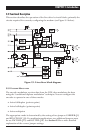
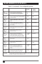
2.2.4 R
ECEIVER
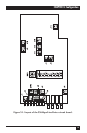
The receiver comprises several circuits, as shown in the block diagram (see
Figure 2-1):
• The RECEIVE FILTER, which removes all the out-band frequencies.
• The EQUALIZER, which comprises several equalizers activated according to
data rate.
• The digital Automatic Gain Control (AGC), which automatically compensates
for the attenuation of the line.