


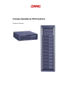

3
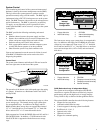
Architecture
The traditional bus interconnect has been replaced by a switch-
based interconnect system. With a bus design, the processors,
memory, and I/O modules share the bus. As the number of bus
users increases, the transactions interfere with one another,
increasing latency and decreasing aggregate bandwidth.
However, with a switch-based system there is no degradation
in performance as the number of CPUs, memory, and I/O users
increase. Although the users increase, the speed is maintained.
With a switch-based, or point-to-point interconnect, the
performance remains constant, even though the number of
transactions multiplies. The switched system interconnect uses
a set of complex chips that route the traffic over multiple paths.
The chipset consists of one C-chip, one P-chip, and two D-
chips.
• C-chip. Provides the command interface from the CPU.
• D-chips. Provide the data path for the CPU, main
memory, and I/O.
• P-chip. Provides the interface to the PCI bus.
This chipset, similar to those used in the AlphaServer DS20
and ES40 systems, supports up to one CPU and up to 2 Gbytes
memory. Interleaving occurs when at least two memory arrays
are used.
The PAD bus, the interface between the P-chip and the D-
chips, is 32 data bits with 4 check bits. The 128-bit memory
bus supports two memory arrays, yielding a 1.3 Gbyte/sec
system bandwidth. Transactions are ECC protected. Upon the
receipt of data, the receiver checks for data integrity and
corrects any errors.
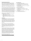
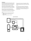
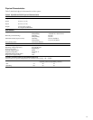
System Block Diagram
C-chip
2 D-chips
P-chip
64 bit PCI
Command, Address, and Control lines for each Memory Array
Control lines for D-chips
Memory
Data Bus
CPU
Data Bus
CAP Bus
PAD
Bus
PKW
1400B-99
CPU
B-cache
1 or 2
Memory
Arrays