


CY14B101L
Document Number: 001-06400 Rev. *I Page 2 of 18
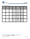
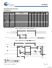
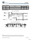
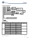
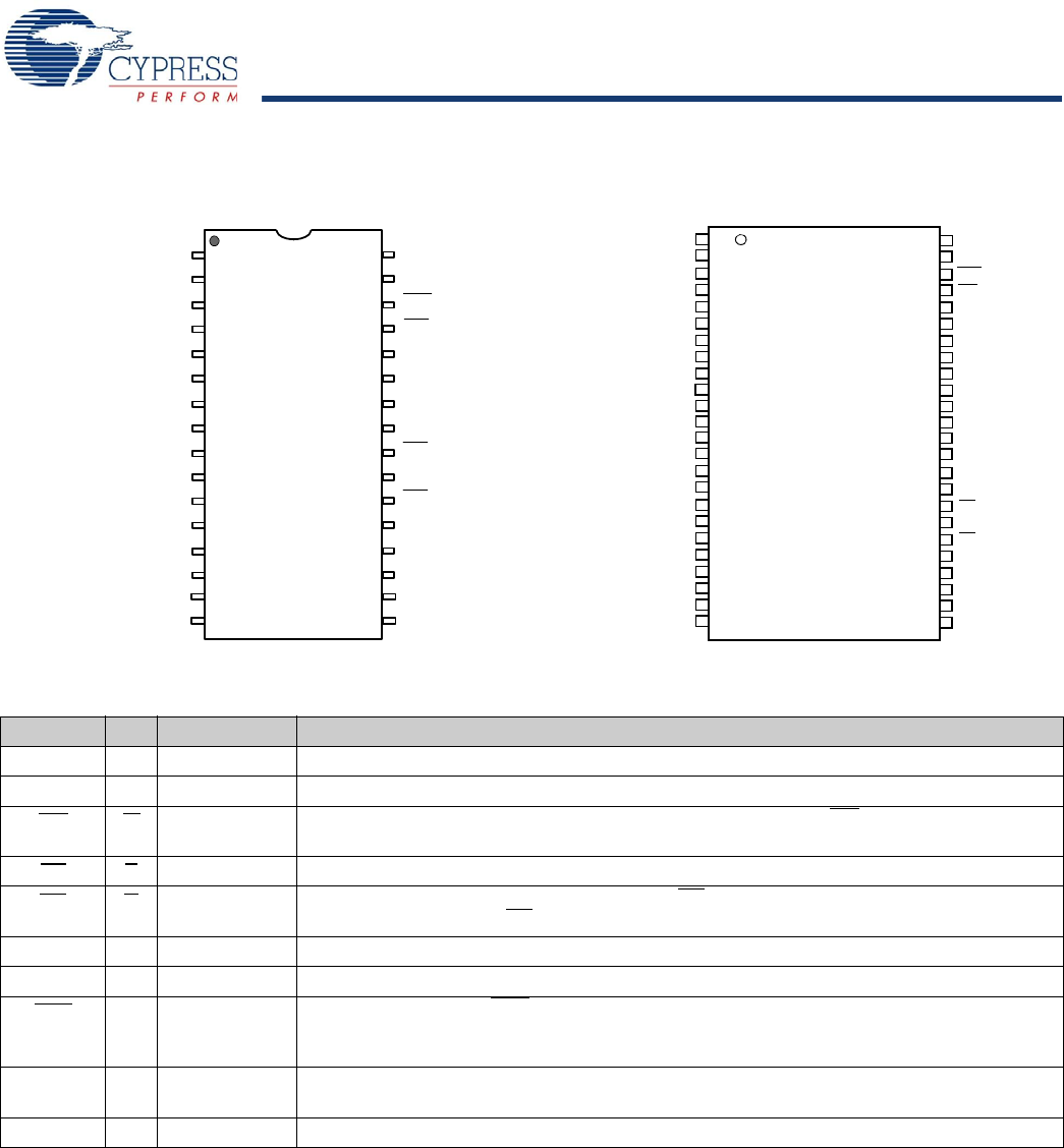
Pinouts
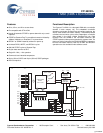
Figure 1. Pin Diagram - 32-Pin SOIC and 48-Pin SSOP
Pin Definitions
Pin Name Alt IO Type Description
A
0
–A
16
Input Address Inputs. Used to select one of the 131,072 bytes of the nvSRAM.
DQ
0
-DQ
7
Input or Output Bidirectional Data IO Lines. Used as input or output lines depending on operation.
WE
W
Input Write Enable Input, Active LOW. When the chip is enabled and WE is LOW, data on the IO
pins is written to the specific address location.
CE
E
Input Chip Enable Input, Active LOW. When LOW, selects the chip. When HIGH, deselects the chip.
OE
G
Input Output Enable, Active LOW. The active LOW OE input enables the data output buffers during
read cycles. Deasserting OE
HIGH causes the IO pins to tri-state.
V
SS
Ground Ground for the Device. The device is connected to ground of the system.
V
CC
Power Supply Power Supply Inputs to the Device.
HSB
Input or Output Hardware Store Busy (HSB). When LOW, this output indicates a Hardware Store is in progress.
When pulled low external to the chip, it initiates a nonvolatile STORE operation. A weak internal
pull up resistor keeps this pin high if not connected (connection optional).
V
CAP
Power Supply AutoStore
Capacitor. Supplies power to nvSRAM during power loss to store data from SRAM
to nonvolatile elements.
NC No Connect No Connect. This pin is not connected to the die.
V
CAP
A
16
A
14
A
12
A
7
A
6
A
5
A
4
A
3
A
2
A
1
A
0
DQ
0
DQ
1
V
CC
A
15
HSB
WE
A
13
A
8
A
9
A
11
OE
A
10
CE
DQ
7
DQ
6
DQ
5
1
2
3
4
5
6
7
8
9
10
11
12
13
14
16
15
V
SS
DQ
2
DQ
3
DQ
4
32
31
30
29
28
27
26
25
24
23
22
21
20
19
18
17
A
16
NC
DQ7
DQ6
DQ5
NC
DQ4
V
CC
DQ3
DQ2
DQ1
DQ0
V
SS
A
0
A
1
A
2
A
3
A
4
A
5
A
6
A
7
NC
HSB
WE
NC
NC
A
8
A
9
A
10
A
11
A
12
A
13
A
14
A
15
1
2
3
4
5
6
7
8
9
10
11
12
13
14
15
16
17
18
19
20
21
22
23
24
25
26
27
28
29
30
31
32
33
34
35
36
37
38
39
40
41
42
43
44
45
46
47
48
Top View
(not to scale)
OE
CE
V
CC
V
SS
V
CAP
NC
NC
NC
NC
NC
NC
NC
NC
NC
[+] Feedback