


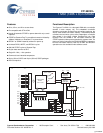
CY14B101L
Document Number: 001-06400 Rev. *I Page 7 of 18
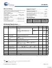
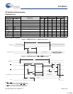
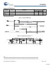
Maximum Ratings
Exceeding maximum ratings may shorten the useful life of the
device. These user guidelines are not tested.
Storage Temperature ................................. –65°C to +150°C
Ambient Temperature with
Power Applied ............................................ –55°C to +125°C
Supply Voltage on V
CC
Relative to GND..........–0.5V to 4.1V
Voltage Applied to Outputs
in High Z State .......................................–0.5V to V
CC
+ 0.5V
Input Voltage...........................................–0.5V to Vcc + 0.5V
Transient Voltage (<20 ns) on
Any Pin to Ground Potential ..................–2.0V to V
CC
+ 2.0V
Package Power Dissipation
Capability (T
A
= 25°C) ...................................................1.0W
Surface Mount Lead Soldering
Temperature (3 Seconds).......................................... +260°C
DC output Current (1 output at a time, 1s duration) ....15 mA
Static Discharge Voltage.......................................... > 2001V
(MIL-STD-883, Method 3015)
Latch Up Current ................................................... > 200 mA
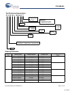
Operating Range
Range Ambient Temperature V
CC
Commercial 0°C to +70°C 2.7V to 3.6V
Industrial -40°C to +85°C 2.7V to 3.6V
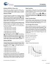
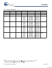
DC Electrical Characteristics
Over the operating range (V
CC
= 2.7V to 3.6V)
[4, 5]
Parameter Description Test Conditions Min Max Unit
I
CC1
Average V
CC
Current t
RC
= 25 ns
t
RC
= 35 ns
t
RC
= 45 ns
Dependent on output loading and cycle rate.
Values obtained without output loads.
I
OUT
= 0 mA.
Commercial 65
55
50
mA
mA
Industrial 70
60
55
mA
mA
mA
I
CC2
Average V
CC
Current
during STORE
All Inputs Do Not Care, V
CC
= Max
Average current for duration t
STORE
6mA
I
CC3
Average V
CC
Current at
t
RC
= 200 ns, 5V, 25°C
Typical
WE
> (V
CC
– 0.2V). All other inputs cycling.
Dependent on output loading and cycle rate. Values obtained
without output loads.
10 mA
I
CC4
Average V
CAP
Current
during AutoStore Cycle
All Inputs Do Not Care, V
CC
= Max
Average current for duration t
STORE
3mA
I
SB
V
CC
Standby Current CE > (V
CC
– 0.2V). All others V
IN
< 0.2V or > (V
CC
– 0.2V).
Standby current level after nonvolatile cycle is complete.
Inputs are static. f = 0 MHz.
3mA
I
IX
Input Leakage Current V
CC
= Max, V
SS
< V
IN
< V
CC
-1 +1 μA
I
OZ
Off State Output
Leakage Current
V
CC
= Max, V
SS
< V
IN
< V
CC
, CE or OE > V
IH
or WE < V
IL
-1 +1 μA
V
IH
Input HIGH Voltage 2.0 V
CC
+
0.5
V
V
IL
Input LOW Voltage V
SS
– 0.5 0.8 V
V
OH
Output HIGH Voltage I
OUT
= –2 mA 2.4 V
V
OL
Output LOW Voltage I
OUT
= 4 mA 0.4 V
V
CAP
Storage Capacitor Between V
CAP
pin and Vss, 6V rated. 17 120 uF
Notes
4. The HSB
pin has I
OUT
= –10 μA for V
OH
of 2.4 V. This parameter is characterized but not tested.
5. V
IH
changes by 100 mV when V
CC
> 3.5V.
[+] Feedback