


PRELIMINARY
CY14B104K, CY14B104M
Document #: 001-07103 Rev. *K Page 14 of 31
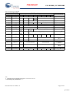
Maximum Ratings
Exceeding maximum ratings may impair the useful life of the
device. These user guidelines are not tested.
Storage Temperature ................................. –65°C to +150°C
Maximum Accumulated Storage Time
At 150°C Ambient Temperature................................... 1000h
At 85°C Ambient Temperature..................... ........... 20 Years
Ambient Temperature with
Power Applied ............................................ –55°C to +150°C
Supply Voltage on V
CC
Relative to GND ..........–0.5V to 4.1V
Voltage Applied to Outputs
in High-Z State....................................... –0.5V to V
CC
+ 0.5V
Input Voltage...........................................–0.5V to Vcc + 0.5V
Transient Voltage (<20 ns) on
Any Pin to Ground Potential .................. –2.0V to V
CC
+ 2.0V
Package Power Dissipation
Capability (T
A
= 25°C) ................................................... 1.0W
Surface Mount Pb Soldering
Temperature (3 Seconds) .......................................... +260°C
DC Output Current (1 output at a time, 1s duration).....15 mA
Static Discharge Voltage.......................................... > 2001V
(per MIL-STD-883, Method 3015)
Latch Up Current ................................................... > 200 mA
Operating Range
Range Ambient Temperature V
CC
Commercial 0°C to +70°C 2.7V to 3.6V
Industrial –40°C to +85°C 2.7V to 3.6V
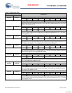
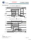
DC Electrical Characteristics
Over the Operating Range (V
CC
= 2.7V to 3.6V)
Parameter Description Test Conditions Min Max Unit
I
CC1
Average V
cc
Current t
RC
= 20 ns
t
RC
= 25 ns
t
RC
= 45 ns
Values obtained without output loads (I
OUT
= 0 mA)
Commercial 65
65
50
mA
mA
Industrial 70
70
52
mA
mA
I
CC2
Average V
CC
Current
during STORE
All Inputs Don’t Care, V
CC
= Max.
Average current for duration t
STORE
10 mA
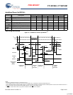
I
CC3
[11]
Average V
CC
Current
at t
RC
= 200 ns, 3V,
25°C typical
All I/P cycling at CMOS levels.
Values obtained without output loads (I
OUT
= 0 mA).
35 mA
I
CC4
Average V
CAP
Current
during AutoStore
Cycle
All Inputs Don’t Care, V
CC
= Max.
Average current for duration t
STORE
5mA
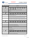
I
SB
V
CC
Standby Current CE > (V
CC
– 0.2V). All others V
IN
< 0.2V or > (V
CC
– 0.2V). Standby
current level after nonvolatile cycle is complete.
Inputs are static. f = 0 MHz.
5mA
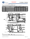
I
IX
[12]
Input Leakage Current
(except HSB
)
V
CC
= Max, V
SS
< V
IN
< V
CC
–1 +1 μA
Input Leakage Current
(for HSB
)
V
CC
= Max, V
SS
< V
IN
< V
CC
–100 +1 μA
I
OZ
Off State Output
Leakage Current
V
CC
= Max, V
SS
< V
OUT
< V
CC
, CE or OE > V
IH
or BHE/BLE > V
IH
or WE < V
IL
–1 +1 μA
V
IH
Input HIGH Voltage 2.0 V
CC
+ 0.5 V
V
IL
Input LOW Voltage V
SS
– 0.5 0.8 V
V
OH
Output HIGH Voltage I
OUT
= –2 mA 2.4 V
V
OL
Output LOW Voltage I
OUT
= 4 mA 0.4 V
V
CAP
[13]
Storage Capacitor Between V
CAP
pin and V
SS
, 5V Rated 61 180 μF
Notes
11. Typical conditions for the active current shown on the DC Electrical characteristics are average values at 25°C (room temperature), and V
CC
= 3V. Not 100% tested.
12. The HSB
pin has I
OUT
= -2 uA for V
OH
of 2.4V when both active HIGH and LOW drivers are disabled. When they are enabled standard V
OH
and V
OL
are valid. This
parameter is characterized but not tested.
13. V
CAP
(Storage capacitor) nominal value is 68uF.
[+] Feedback