


PRELIMINARY
CY14B104K, CY14B104M
Document #: 001-07103 Rev. *K Page 19 of 31
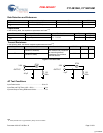
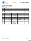
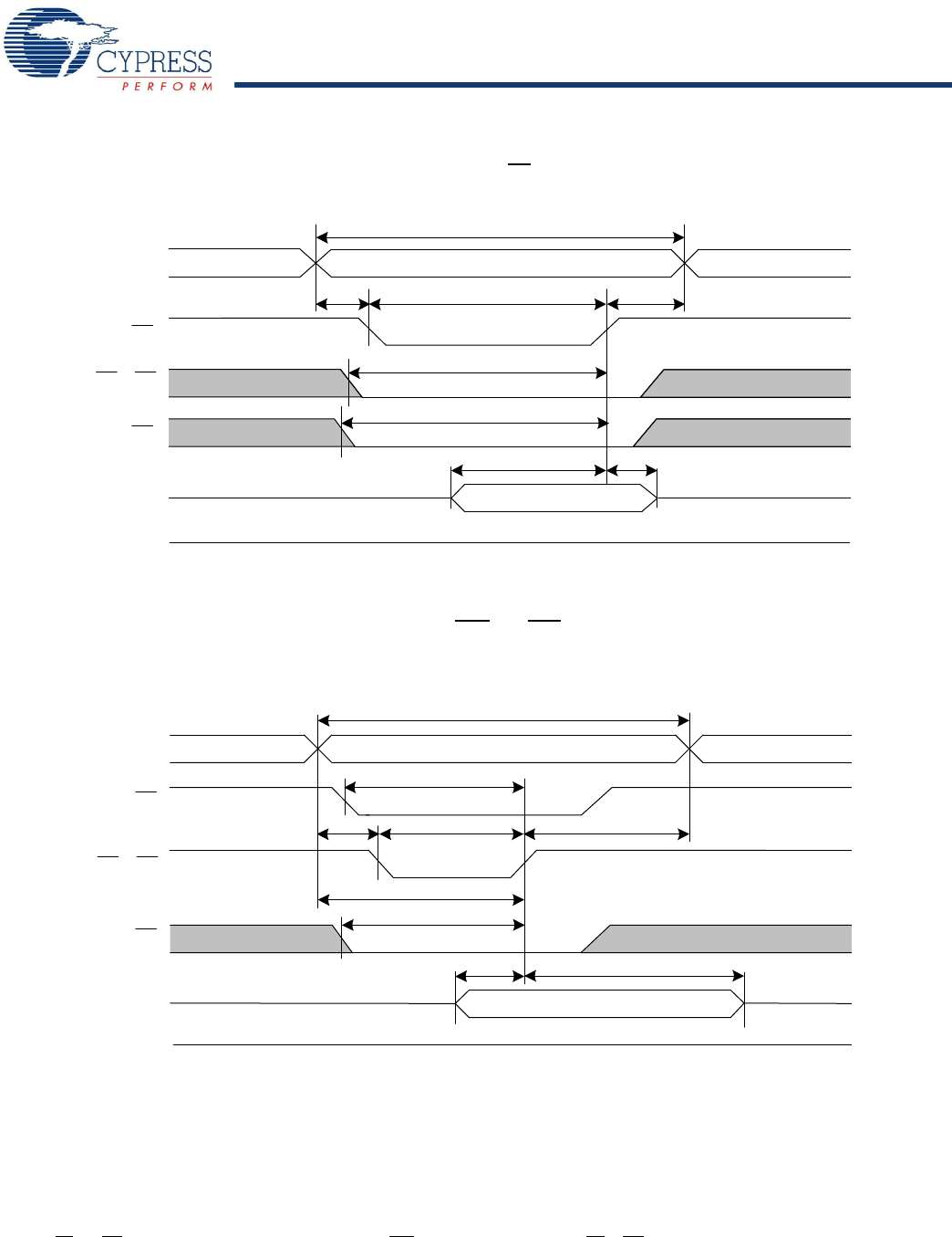
Switching Waveforms
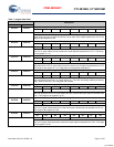
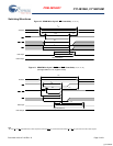
Figure 10. SRAM Write Cycle 2: CE Controlled
[3, 19, 20, 21]
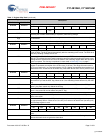
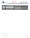
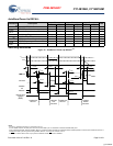
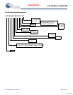
Figure 11. SRAM Write Cycle 3: BHE and BLE Controlled
[6, 19, 20, 21, 22]
Data Output
Data Input
Input Data Valid
High Impedance
Address Valid
Address
t
WC
t
SD
t
HD
BHE, BLE
WE
CE
t
SA
t
SCE
t
HA
t
BW
t
PWE
Data Output
Data Input
Input Data Valid
High Impedance
Address ValidAddress
t
WC
t
SD
t
HD
BHE, BLE
WE
CE
t
SCE
t
SA
t
BW
t
HA
t
AW
t
PWE
(Not applicable for RTC register writes)
Note
22. Only CE
and WE controlled writes to RTC registers are allowed. BLE pin must be held LOW before CE or WE pin goes LOW for writes to RTC register.
[+] Feedback