


CY24272
Document Number: 001-42414 Rev. ** Page 10 of 13
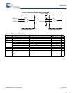
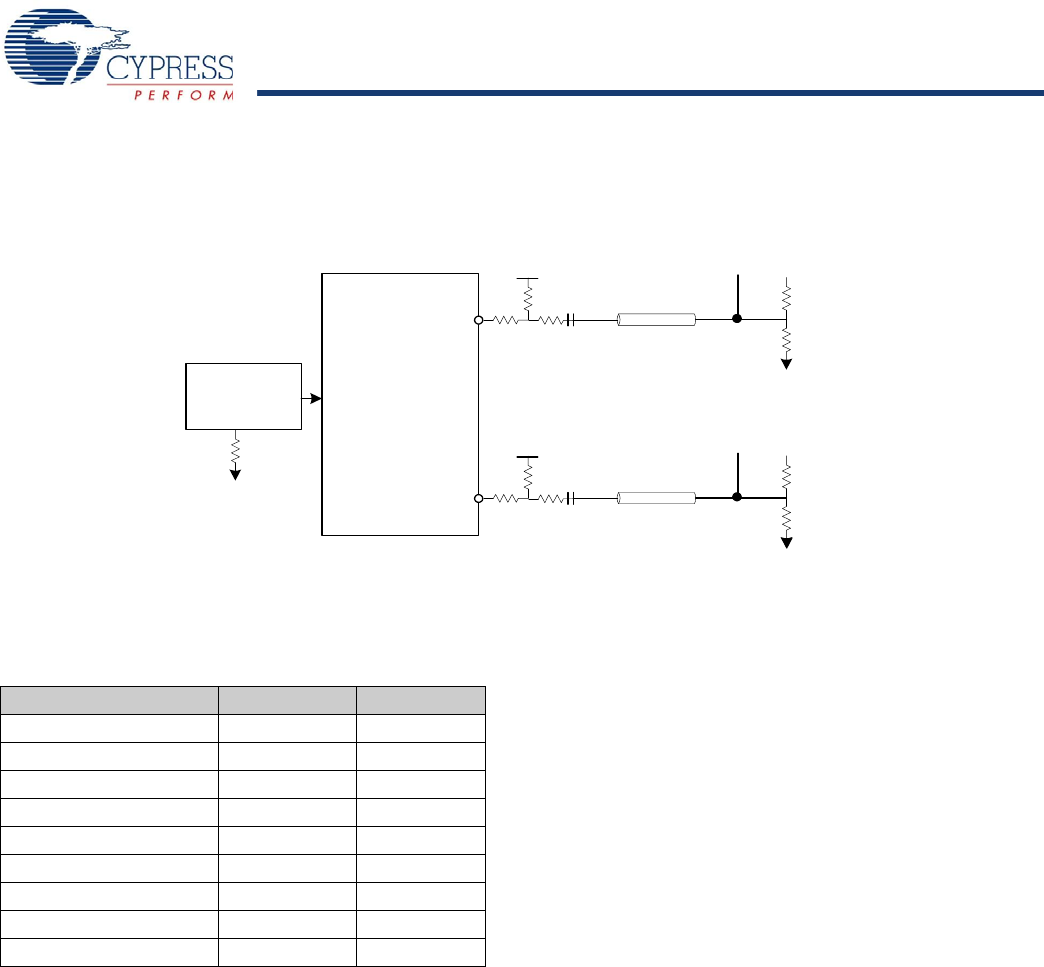
Test and Measurement Setup
Figure 3. Clock Outputs
Signal Waveforms
A physical signal that appears at the pins of a device is deemed
valid or invalid depending on its voltage and timing relations with
other signals. Input and output voltage waveforms are defined as
shown in Figure 4 on page 11. Both rise and fall times are defined
between the 20% and 80% points of the voltage swing, with the
swing defined as V
H
–V
L
.
Figure 5 on page 11 shows the definition of the output crossing
point. The nominal crossing point between the complementary
outputs is defined as the 50% point of the DC voltage levels.
There are two crossing points defined: Vx+ at the rising edge of
CLK and Vx– at the falling edge of CLK. For some waveforms,
both Vx+ and Vx– are below Vx,nom (for example, if t
CR
is larger
than t
CF
).
Jitter
This section defines the specifications that relate to timing uncer-
tainty (or jitter) of the input and output waveforms. Figure 6 on
page 11 shows the definition of cycle-to-cycle jitter with respect
to the falling edge of the CLK signal. Cycle-to-cycle jitter is the
difference between cycle times of adjacent cycles. Equal require-
ments apply rising edges of the CLK signal. Figure 7 on page 11
shows the definition of cycle-to-cycle duty cycle error (t
DC,ERR
).
Cycle-to-cycle duty cycle is defined as the difference between
t
PW+
(high times) of adjacent differential clock cycles. Equal
requirements apply to t
PW-
, low times of the differential click
cycles.
Differential Driver
CLK
CLKB
Swing Current
Control
ISET
R
RC
Measurement
Point
V
TS
R
1
Z
CH
V
T
R
T1
C
S
R
T2
R
3
R
2
Measurement
Point
V
TS
R
1
Z
CH
V
T
R
T1
C
S
R
T2
R
3
R
2
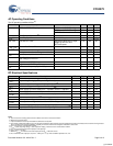
Notes
19.Max and min output clock cycle times are based on nominal outputs frequency of 300 and 667 MHz, respectively. For spread spectrum modulated differential or
single-ended REFCLK, the output clock tracks the modulation of the input.
20.Output short term jitter spec is the absolute value of the worst case deviation.
21.t
SKEW
is the timing difference between any two of the four differential clocks and is measured at common mode voltage. Δt
SKEW
is the change in t
SKEW
when the
operating temperature and supply voltage change.
22.t
CR,CF
applies only when appropriate R
RC
and output resistor network resistor values are selected to match pull up and pull down currents.
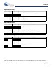
Example External Resistor Values
and Termination Voltages for a 50Ω Channel
Parameter Value Unit
R
1
33.0 Ω
R
2
18.0 Ω
R
3
17.0 Ω
R
T1
60.4 Ω
R
T2
301 Ω
C
S
2700 pF
R
RC
432 Ω
V
TS
2.5V V
V
T
1.2V V
[+] Feedback