


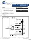
CY24272
Document Number: 001-42414 Rev. ** Page 7 of 13
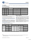
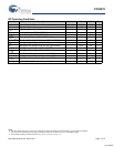
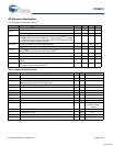
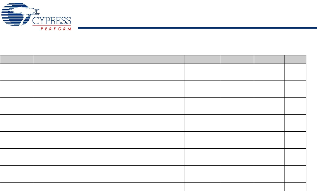
DC Operating Conditions
Parameter Description Condition Min Max Unit
V
DDP
Supply Voltage for PLL 2.5V ± 5% 2.375 2.625 V
V
DDC
Supply Voltage for Core 2.5V ± 5% 2.375 2.625 V
V
DD
Supply Voltage for Clock Buffers 2.5V ± 5% 2.375 2.625 V
V
IHCLK
Input High Voltage, REFCLK/REFCLKB 0.6 0.95 V
V
ILCLK
Input Low Voltage, REFCLK/REFCLKB –0.15 +0.15 V
V
IXCLK
[6]
Crossing Point Voltage, REFCLK/REFCLKB 200 550 mV
ΔV
IXCLK
[6]
Difference in Crossing Point Voltage, REFCLK/REFCLKB – 150 mV
V
IH
Input Signal High Voltage at ID0, ID1, EN, and /BYPASS 1.4 2.625 V
V
IL
Input Signal Low Voltage at ID0, ID1, EN, and /BYPASS –0.15 0.8 V
V
IH,SM
Input Signal High Voltage at SCL and SDA
[7]
1.4 3.465 V
V
IL,SM
Input Signal Low Voltage at SCL and SDA –0.15 0.8 V
V
TH
[8]
Input Threshold Voltage for single-ended REFCLK 0.35 0.5V
DD
V
V
IH,SE
Input Signal High Voltage for single-ended REFCLK V
TH
+ 0.3 2.625 V
V
IL,SE
Input Signal Low Voltage for single-ended REFCLK –0.15 V
TH
– 0.3 V
T
A
Ambient Operating Temperature 0 70 °C
Notes
6. Not 100% tested except V
IXCLK
and ΔV
IXCLK
. Parameters guaranteed by design and characterizations, not 100% tested in production.
7. This range of SCL and SDA input high voltage enables the CY24272 for use with 3.3V, 2.5V, or 1.8V SMBus voltages.
8. Single-ended operation guaranteed only when 0.8 < (V
IH,SE
– V
TH
)/(V
TH
– V
IL
,
SE
) < 1.2.
[+] Feedback