


CY24272
Document Number: 001-42414 Rev. ** Page 2 of 13
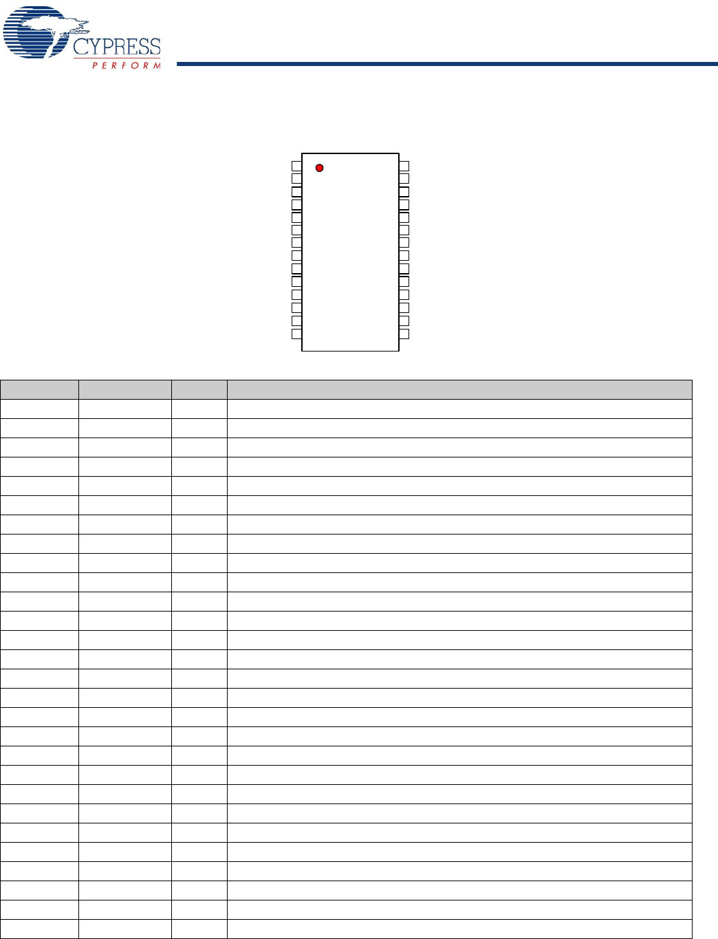
Pinouts
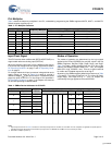
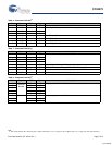
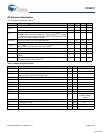
Table 2. Pin Definition - 28 Pin TSSOP
Pin No. Name IO Description
1 VDDP PWR 2.5V power supply for phased lock loop (PLL)
2 VSSP GND Ground
3 ISET I Set clock driver current (external resistor)
4 VSS GND Ground
5 REFCLK I Reference clock input (connect to clock source)
6 REFCLKB I Complement of reference clock (connect to clock source)
7 VDDC PWR 2.5V power supply for core
8 VSSC GND Ground
9 SCL I SMBus clock (connect to SMBus)
10 SDA I SMBus data (connect to SMBus)
11 EN I Output Enable (CMOS signal)
12 ID0 I Device ID (CMOS signal)
13 ID1 I Device ID (CMOS signal)
14 /BYPASS I REFCLK bypassing PLL (CMOS signal)
15 VDD PWR Power supply for outputs
16 CLK3B O Complement clock output
17 CLK3 O Clock output
18 VSS GND Ground
19 CLK2B O Complement clock output
20 CLK2 O Clock output
21 VSS GND Ground
22 VDD PWR Power supply for outputs
23 CLK1B O Complement clock output
24 CLK1 O Clock output
25 VSS GND Ground
26 CLK0B O Complement clock output
27 CLK0 O Clock output
28 VDD PWR Power supply for outputs
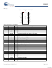
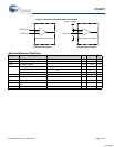
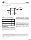
Figure 1. Pin Diagram - 28 Pin TSSOP
/BYPASS
REFCLKB
VDD
CLK0B
VSS
CLK2B
CLK3
CLK3B
VDD
VSS
CLK2
CLK0
VSS
CLK1
CLK1B
VDD
VDDP
ISET
VSSC
SDA
ID0
ID1
EN
SCL
VSSP
VSS
REFCLK
VDDC
1
2
3
4
5
6
7
8
9
10
11
12
13
14
28
27
26
25
24
23
22
21
20
19
18
17
16
15
CY24272
[+] Feedback