


MoBL
®
CY62128E
Document #: 38-05485 Rev. *F Page 3 of 12
Maximum Ratings
Exceeding maximum ratings may impair the useful life of the
device. These user guidelines are not tested.
Storage Temperature ................................. –65°C to +150°C
Ambient Temperature with
Power Applied ............................................ –55°C to +125°C
Supply Voltage to Ground
Potential...............................–0.5V to 6.0V (V
CC(max)
+ 0.5V)
DC Voltage Applied to Outputs
in High-Z State
[5, 6]
..............–0.5V to 6.0V (V
CC(max)
+ 0.5V)
DC Input Voltage
[5, 6]
...........–0.5V to 6.0V (V
CC(max)
+ 0.5V)
Output Current into Outputs (LOW)............................. 20 mA
Static Discharge Voltage...........................................> 2001V
(MIL-STD-883, Method 3015)
Latch up Current.....................................................> 200 mA
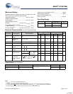
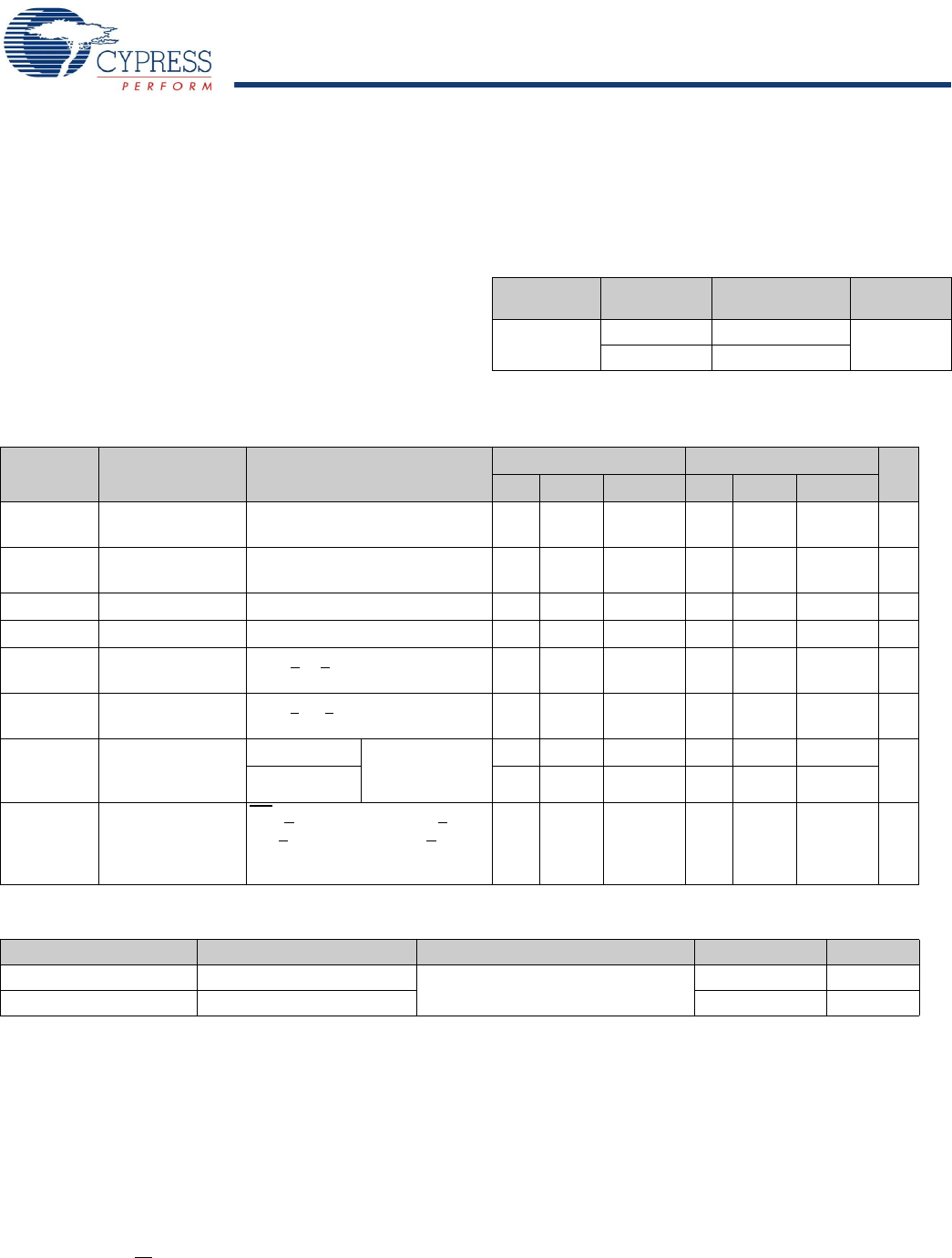
Operating Range
Device Range
Ambient
Temperature
V
CC
[7]
CY62128ELL Ind’l/Auto-A –40°C to +85°C 4.5V to 5.5V
Auto-E –40°C to +125°C
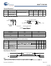
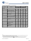
Electrical Characteristics (Over the Operating Range)
Parameter Description Test Conditions
45 ns (Ind’l/Auto-A) 55 ns (Auto-E)
Unit
Min Typ
[3]
Max Min Typ
[3]
Max
V
OH
Output HIGH
Voltage
I
OH
= –1 mA 2.4 2.4 V
V
OL
Output LOW
Voltage
I
OL
= 2.1 mA 0.4 0.4 V
V
IH
Input HIGH Voltage V
CC
= 4.5V to 5.5V 2.2 V
CC
+ 0.5 2.2 V
CC
+ 0.5 V
V
IL
Input LOW voltage V
CC
= 4.5V to 5.5V –0.5 0.8 –0.5 0.8 V
I
IX
Input Leakage
Current
GND < V
I
< V
CC
–1 +1 –4 +4 μA
I
OZ
Output Leakage
Current
GND < V
O
< V
CC
, Output Disabled –1 +1 –4 +4 μA
I
CC
V
CC
Operating
Supply Current
f = f
max
= 1/t
RC
V
CC
= V
CC(max)
I
OUT
= 0 mA
CMOS levels
11 16 11 35 mA
f = 1 MHz 1.3 2 1.3 4
I
SB2
[8]
Automatic CE
Power down
Current—CMOS
Inputs
CE
1
> V
CC
– 0.2V or CE
2
< 0.2V,
V
IN
> V
CC
– 0.2V or V
IN
< 0.2V,
f = 0, V
CC
= V
CC(max)
14 130μA
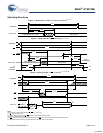
Capacitance (For all Packages)
[9]
Parameter Description Test Conditions Max Unit
C
IN
Input Capacitance T
A
= 25°C, f = 1 MHz,
V
CC
= V
CC(typ)
10 pF
C
OUT
Output Capacitance 10 pF
Notes
5. V
IL(min)
= –2.0V for pulse durations less than 20 ns.
6. V
IH(max)
= V
CC
+ 0.75V for pulse durations less than 20 ns.
7. Full device AC operation assumes a 100 μs ramp time from 0 to V
CC
(min) and 200 μs wait time after V
CC
stabilization.
8. Only chip enables (CE
1
and CE
2
) must be at CMOS level to meet the I
SB2
/ I
CCDR
spec. Other inputs can be left floating.
9. Tested initially and after any design or process changes that may affect these parameters.
[+] Feedback