


MoBL
®
CY62128E
Document #: 38-05485 Rev. *F Page 4 of 12
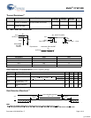
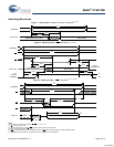
AC Test Loads and Waveform
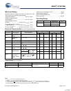
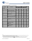
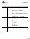
Thermal Resistance
[9]
Parameter Description Test Conditions
SOIC
Package
STSOP
Package
TSOP
Package
Unit
Θ
JA
Thermal Resistance
(Junction to Ambient)
Still Air, soldered on a 3 × 4.5 inch,
two-layer printed circuit board
48.67 32.56 33.01 °C/W
Θ
JC
Thermal Resistance
(Junction to Case)
25.86 3.59 3.42 °C/W
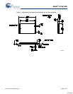
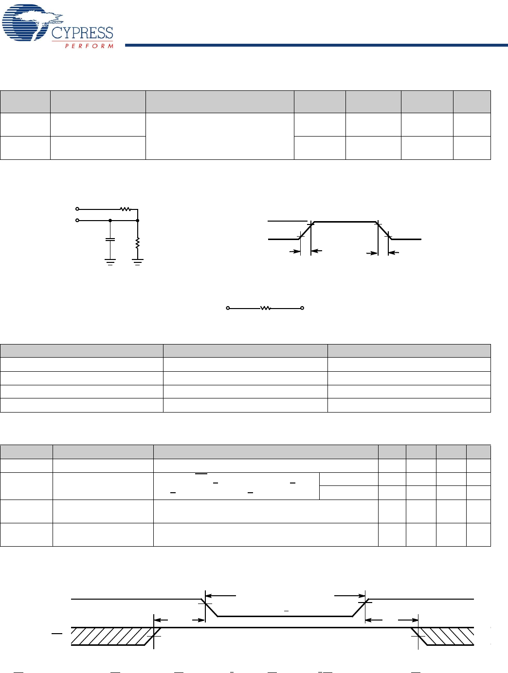
3.0V
V
CC
OUTPUT
R2
30 pF
INCLUDING
JIG AND
SCOPE
GND
90%
10%
90%
10%
Rise Time = 1 V/ns
Fall Time = 1 V/ns
OUTPUT V
Equivalent to: THEVENIN EQUIVALENT
ALL INPUT PULSES
R
TH
R1
Parameters Value Unit
R1 1800 Ω
R2 990 Ω
R
TH
639 Ω
V
TH
1.77 V
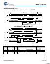
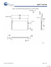
Data Retention Characteristics (Over the Operating Range)
Parameter Description Conditions Min Typ
[3]
Max Unit
V
DR
V
CC
for Data Retention 2 V
I
CCDR
[8]
Data Retention Current V
CC
= V
DR
, CE
1
> V
CC
− 0.2V or CE
2
< 0.2V,
V
IN
> V
CC
- 0.2V or V
IN
< 0.2V
Ind’l/Auto-A 4 μA
Auto-E 30 μA
t
CDR
[9]
Chip Deselect to Data
Retention Time
0ns
t
R
[10]
Operation Recovery
Time
t
RC
ns
Data Retention Waveform
[11]
V
CC(min)
V
CC(min)
t
CDR
V
DR
> 2.0V
DATA RETENTION MODE
t
R
V
CC
CE
Notes
10.Full device AC operation requires linear V
CC
ramp from V
DR
to V
CC(min)
> 100 μs or stable at V
CC(min)
> 100 μs.
11. CE
is the logical combination of CE
1
and CE
2
. When CE
1
is LOW and CE
2
is HIGH, CE is LOW; when CE
1
is HIGH or CE
2
is LOW, CE is HIGH.
Notes
10.Full device AC operation requires linear V
CC
ramp from V
DR
to V
CC(min)
> 100 μs or stable at V
CC(min)
> 100 μs.
11. CE
is the logical combination of CE
1
and CE
2
. When CE
1
is LOW and CE
2
is HIGH, CE is LOW; when CE
1
is HIGH or CE
2
is LOW, CE is HIGH.
[+] Feedback