Document Number: 38-07138 Rev. *B Page 14 of 19
range since the highest frequency output is running at 20 MHz.
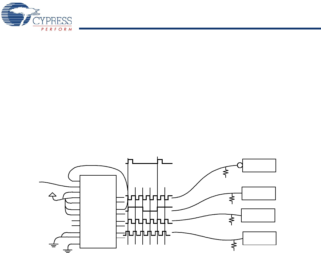
Figure 7 shows some of the functions that are selectable on the
3Qx and 4Qx outputs. These include inverted outputs and
outputs that offer divide-by-2 and divide-by-4 timing. An inverted
output enables the system designer to clock different
subsystems on opposite edges, without suffering from the pulse
asymmetry typical of non-ideal loading. This function enables
each of the two subsystems to clock 180 degrees out of phase
and align within the skew specifications.
The divided outputs offer a zero delay divider for portions of the
system that need the clock divided by either two or four, and still
remain within a narrow skew of the “1X” clock. Without this
feature, an external divider is added, and the propagation delay
of the divider adds to the skew between the different clock
signals.
These divided outputs, coupled with the Phase Locked Loop,
enables the PSCB to multiply the clock rate at the REF input by
either two or four. This mode enables the designer to distribute
a low frequency clock between various portions of the system,
and then locally multiply the clock rate to a more suitable
frequency, still maintaining the low skew characteristics of the
clock driver. The PSCB performs all of the functions described in
this section at the same time. It multiplies by two and four or
divides by two (and four) at the same time. In other words, it is
shifting its outputs over a wide range or maintaining zero skew
between selected outputs.
Figure 7. Multi-Function Clock Driver
20 MHz
DISTRIBUTION
CLOCK
80 MHz
INVERTED
Z
0
20 MHz
80 MHz
ZERO SKEW
80 MHz
SKEWED –3.125 ns (–4t
U
)
FB
REF
FS
4F0
4F1
3F0
3F1
2F0
2F1
1F0
1F1
4Q0
4Q1
3Q0
3Q1
2Q0
2Q1
1Q0
1Q1
TEST
REF
LOAD
LOAD
LOAD
LOAD
Z
0
Z
0
Z
0
[+] Feedback


