


CY7B991
CY7B992
Document Number: 38-07138 Rev. *B Page 15 of 19
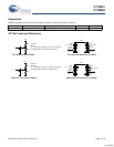
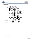
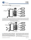
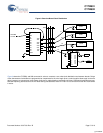
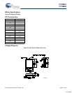
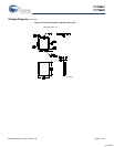
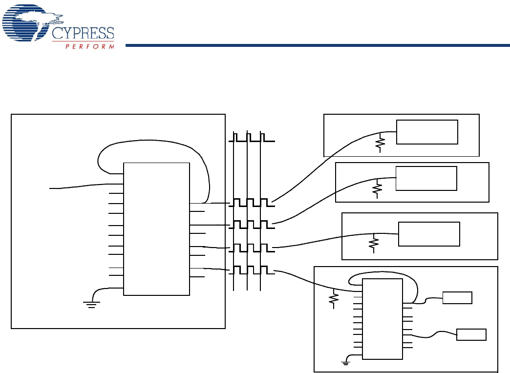
Figure 8 shows the CY7B991 and 992 connected in series to construct a zero skew clock distribution tree between boards. Delays
of the downstream clock buffers are programmed to compensate for the wire length (that is, select negative skew equal to the wire
delay) necessary to connect them to the master clock source, approximating a zero delay clock tree. Cascaded clock buffers accumu-
lates low frequency jitter because of the non-ideal filtering characteristics of the PLL filter. Do not connect more than two clock buffers
in series.
Figure 8. Board-to-Board Clock Distribution
SYSTEM
CLOCK
Z
0
L1
L2
L3
L4
FB
REF
FS
4F0
4F1
3F0
3F1
2F0
2F1
1F0
1F1
4Q0
4Q1
3Q0
3Q1
2Q0
2Q1
1Q0
1Q1
TEST
REF
4F0
4F1
3F0
3F1
2F0
2F1
1F0
1F1
4Q0
4Q1
3Q0
3Q1
2Q0
2Q1
1Q0
1Q1
REF
FS
FB
LOAD
LOAD
LOAD
LOAD
LOAD
TEST
Z
0
Z
0
Z
0
[+] Feedback