


CY7C0850AV, CY7C0851AV
CY7C0852AV, CY7C0853AV
Document #: 38-06070 Rev. *H Page 18 of 32
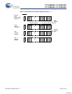
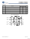
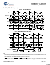
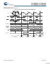
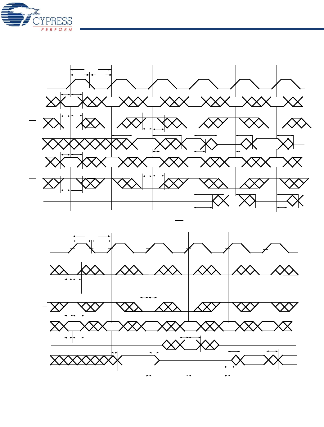
Figure 10. Bank Select Read
[26, 27]
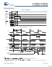
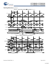
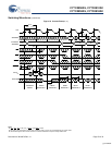
Figure 11. Read-to-Write-to-Read (OE = LOW)
[25, 28, 29, 30, 31]
Switching Waveforms (continued)
Q
3
Q
1
Q
0
Q
2
A
0
A
1
A
2
A
3
A
4
A
5
Q
4
A
0
A
1
A
2
A
3
A
4
A
5
t
SA
t
HA
t
SC
t
HC
t
SA
t
HA
t
SC
t
HC
t
SC
t
HC
t
SC
t
HC
t
CKHZ
t
DC
t
DC
t
CD2
t
CKLZ
t
CD2
t
CD2
t
CKHZ
t
CKLZ
t
CD2
t
CKHZ
t
CKLZ
t
CD2
t
CH2
t
CL2
t
CYC2
CLK
ADDRESS
(B1)
CE
(B1)
DATA
OUT(B2)
DATA
OUT(B1)
ADDRESS
(B2)
CE
(B2)
t
CYC2
t
CL2
t
CH2
t
HC
t
SC
t
HW
t
SW
t
HA
t
SA
t
HW
t
SW
t
CD2
t
CKHZ
t
SD
t
HD
NO
OPERATION WRITEREAD READ
CLK
CE
R/W
ADDRESS
DATA
IN
DATA
OUT
A
n
A
n+1
A
n+2
A
n+2
D
n+2
A
n+3
A
n+4
Q
n
Q
n+3
Q
n+1
t
CD2
t
CD2
t
CKLZ
Notes
26.In this depth-expansion example, B1 represents Bank #1 and B2 is Bank #2; each bank consists of one Cypress CY7C0851AV/CY7C0852AV device from this data
sheet. ADDRESS
(B1)
= ADDRESS
(B2)
.
27. ADS
= CNTEN= B0 – B3 = OE = LOW; MRST = CNTRST = CNT/MSK = HIGH.
28.Output state (HIGH, LOW, or high-impedance) is determined by the previous cycle control signals.
29.During “No Operation,” data in memory at the selected address may be corrupted and should be rewritten to ensure data integrity.
30. CE
0
= OE = B0 – B3 = LOW; CE
1
= R/W = CNTRST = MRST = HIGH.
31.CE
0
= B0 – B3 = R/W = LOW; CE
1
= CNTRST = MRST = CNT/MSK = HIGH. When R/W first switches low, since OE = LOW, the Write operation cannot be completed
(labelled as no operation). One clock cycle is required to three-state the I/O for the Write operation on the next rising edge of CLK.
[+] Feedback