CY7C0850AV, CY7C0851AV
CY7C0852AV, CY7C0853AV
Document #: 38-06070 Rev. *H Page 31 of 32
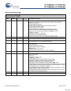
Document History Page
Document Title: CY7C0850AV/CY7C0851AV/CY7C0852AV/CY7C0853AV, FLEx36™ 3.3V 32K/64K/128K/256K x 36
Synchronous Dual-Port RAM
Document Number: 38-06070
REV. ECN NO.
Submis-
sion Date
Orig. of
Change
Description of Change
** 127809 08/04/03 SPN This data sheet has been extracted from another data sheet: the 2M/4M/9M
data sheet. The following changes have been made from the original as
pertains to this device:
Updated capacitance values
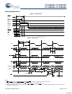
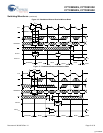
Updated “Read-to-Write-to-Read (OE Controlled)” waveform
Revised static discharge voltage
Corrected 0853 pins L3 and L12
Added discussion of Pause/Restart for JTAG boundary scan
Power up requirements added to Maximum Ratings information
Revise t
cd2, tOE, tOHZ, tCKHZ, tCKLZ for the CY7C0853V to 4.7 ns
Updated I
cc numbers
Updated t
HA, tHB, tHD for -100 speed
Separated out from the 4M data sheet
Added 133-MHz Industrial device to Ordering Information table
*A 210948 See ECN YDT Changed mailbox addresses from 1FFFE and 1FFFF to 3FFFE and 3FFFF.
*B 216190 See ECN YDT/Dcon Corrected Revision of Document. CMS does not reflect this rev change
*C 231996 See ECN YDT Removed “A particular port can write to a certain location while another port is
reading that location.” from Functional Description.
*D 238938 See ECN WWZ Merged 0853 (9Mx36) with 0852 (4Mx36) and 0851(2Mx36), add 0850 (1M x36),
to the data sheet.
Added product selection table.
Added JTAG ID code for 1M device.
Added note 14.
Updated boundary scan section.
Updated function description for the merge and addition.
*E 329122 See ECN SPN Updated Marketing part numbers
*F 389877 See ECN KGH Updated Read-to-Write-to-Read timing diagram to reflect accurate bus
turnaround scheme.
Added I
SB5
Changed t
RSCNTINT
to 10ns
Changed t
RSF
to 10ns
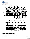
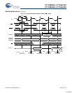
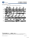
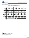
Added figure Disabled-to-Read-to-Read-to-Read-to-Write
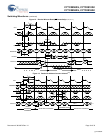
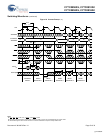
Added figure Disabled-to-Write-to-Read-to-Write-to-Read
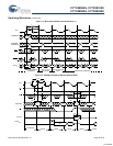
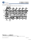
Added figure Disabled-to-Read-to-Disabled-to-Write
Added figure Read-to-Readback-to-Read-to-Read (R/W
= HIGH)
Updated Read-to-Write-to-Read timing diagram to correct the data out schemes
Updated Disabled-to-Read-to-Read-to-Read-to-Write timing diagram to correct
the chip enable, data in, and data out schemes
Updated Disabled-to-Write-to-Read-to-Write-to-Read timing diagram to correct
the chip enable and output enable schemes
Updated Disabled-to-Read-to-Disabled-to-Write timing diagram to correct the
chip enable and output enable schemes
*G 391597 See ECN SPN Updated counter reset section to reflect mirror register behavior
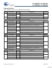
*H 2544945 07/29/08 VKN/AESA Updated Template. Updated ordering information
[+] Feedback


