


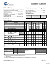
CY7C0850AV, CY7C0851AV
CY7C0852AV, CY7C0853AV
Document #: 38-06070 Rev. *H Page 7 of 32
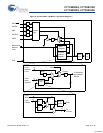
Master Reset
The FLEx36 family devices undergo a complete reset by taking
its MRST
input LOW. The MRST input can switch asynchro-
nously to the clocks. The MRST
initializes the internal burst
counters to zero, and the counter mask registers to all ones
(completely unmasked). The MRST
also forces the Mailbox
Interrupt (INT
) flags and the Counter Interrupt (CNTINT) flags
HIGH. The MRST
must be performed on the FLEx36 family
devices after power up.
Mailbox Interrupts
The upper two memory locations may be used for message
passing and permit communications between ports. Table 2
shows the interrupt operation for both ports of CY7C0853AV.
The highest memory location, 3FFFF is the mailbox for the right
port and 3FFFE is the mailbox for the left port. Table 2 shows that
in order to set the INT
R
flag, a Write operation by the left port to
address 3FFFF asserts INT
R
LOW. At least one byte has to be
active for a Write to generate an interrupt. A valid Read of the
3FFFF location by the right port resets INT
R
HIGH. At least one
byte has to be active in order for a Read to reset the interrupt.
When one port Writes to the other port’s mailbox, the INT of the
port that the mailbox belongs to is asserted LOW. The INT
is
reset when the owner (port) of the mailbox Reads the contents
of the mailbox. The interrupt flag is set in a flow-thru mode (i.e.,
it follows the clock edge of the writing port). Also, the flag is reset
in a flow-thru mode (i.e., it follows the clock edge of the reading
port).
Each port can read the other port’s mailbox without resetting the
interrupt. And each port can write to its own mailbox without
setting the interrupt. If an application does not require message
passing, INT
pins should be left open.
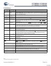
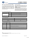
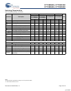
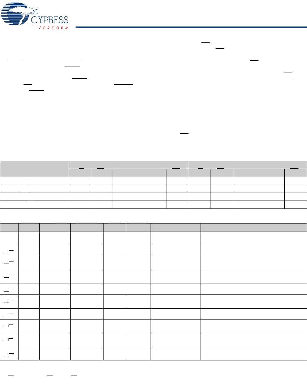
Table 2. Interrupt Operation Example
[1, 4, 5, 6, 7]
Function
Left Port Right Port
R/W
L
CE
L
A
0L–17L
INT
L
R/W
R
CE
R
A
0R–17R
INT
R
Set Right INT
R
Flag L L 3FFFF X X X X L
Reset Right INT
R
Flag X X X X H L 3FFFF H
Set Left INT
L
Flag X X X L L L 3FFFE X
Reset Left INT
L
Flag H L 3FFFE H X X X X
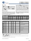
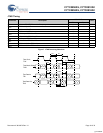
Table 3. Address Counter and Counter-Mask Register Control Operation (Any Port)
[8, 9]
CLK MRST CNT/MSK CNTRST ADS CNTEN Operation Description
X L X X X X Master Reset Reset address counter to all 0s and mask
register to all 1s.
H H L X X Counter Reset Reset counter unmasked portion to all 0s.
H H H L L Counter Load Load counter with external address value
presented on address lines.
H H H L H Counter Readback Read out counter internal value on address
lines.
H H H H L Counter Increment Internally increment address counter value.
H H H H H Counter Hold Constantly hold the address value for
multiple clock cycles.
H L L X X Mask Reset Reset mask register to all 1s.
H L H L L Mask Load Load mask register with value presented on
the address lines.
H L H L H Mask Readback Read out mask register value on address
lines.
H L H H X Reserved Operation undefined
Notes
4. CE
is internal signal. CE = LOW if CE
0
= LOW and CE
1
= HIGH. For a single Read operation, CE only needs to be asserted once at the rising edge of the CLK and
can be deasserted after that. Data is out after the following CLK edge and is three-stated after the next CLK edge.
5. OE
is “Don’t Care” for mailbox operation.
6. At least one of B0
, B1, B2, or B3 must be LOW.
7. A16x is a NC for CY7C0851AV, therefore the Interrupt Addresses are FFFF and EFFF; A16x and A15x are NC for CY7C0850AV, therefore the Interrupt Addresses
are 7FFF and 6FFF.
8. “X” = “Don’t Care,” “H” = HIGH, “L” = LOW.
9. Counter operation and mask register operation is independent of chip enables.
[+] Feedback