CY7C1307BV25
CY7C1305BV25
Document #: 38-05630 Rev. *A Page 21 of 21
Document History Page
Document Title: CY7C1305BV25/CY7C1307BV25 18-Mbit Burst of Four Pipelined SRAM with QDR™ Architecture
Document Number: 38-05630
REV. ECN NO. Issue Date
Orig. of
Change Description of Change
** 253049 See ECN SYT New Data Sheet
*A 436864 See ECN NXR Converted from Preliminary to Final.
Removed 133 MHz & 100 MHz from product offering.
Included industrial Operating Range.
Changed C/C
Description in the Features Section & Pin Description Table.
Changed t
TCYC
from 100 ns to 50 ns, changed t
TF
from 10 MHz to 20 MHz
and changed t
TH
and t
TL
from 40 ns to 20 ns in TAP AC Switching
Characteristics table
Modified the ZQ pin definition as follows:
Alternately, this pin can be connected directly to V
DDQ
, which enables the
minimum impedance mode
Included Maximum Ratings for Supply Voltage on V
DDQ
Relative to GND
Changed the Maximum Ratings for DC Input Voltage from V
DDQ
to V
DD.
Modified the Description of I
X
from Input Load current to Input Leakage
Current on page # 16.
Modified test condition in note# 16 from V
DDQ
< V
DD
to
V
DDQ
≤ V
DD
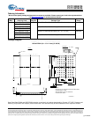
Updated the Ordering Information table and replaced the Package Name
Column with Package Diagram.
[+] Feedback


