CY7C604XX
Document Number: 001-12395 Rev *H Page 15 of 30
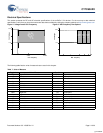
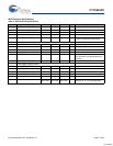
ADC Electrical Specifications
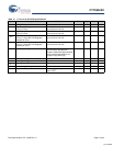
Table 8. ADC Electrical Specifications
Symbol Description Min Typ Max Units Conditions
Input
Input Voltage Range Vss 1.3 V This gives 72% of maximum code
Input Capacitance 5 pF
Resolution 8 Bits
8-Bit Sample Rate 23.4375 ksps Data Clock set to 6 MHz. Sample Rate
= 0.001/(2^Resolution/Data clock)
DC Accuracy
DNL -1 +2 LSb For any configuration
INL -2 +2 LSb For any configuration
Offset Error 0 15 90 mV
Operating Current 275 350 μA
Data Clock 2.25 12 MHz Source is chip’s internal main oscillator.
See AC Chip Level Specifications for
accuracy.
Monotonicity Not guaranteed. See DNL
Power Supply Rejection Ratio
PSRR (Vdd>3.0V) 24 dB
PSRR (2.2 < Vdd < 3.0) 30 dB
PSRR (2.0 < Vdd < 2.2) 12 dB
PSRR (Vdd < 2.0) 0 dB
Gain Error 1 5 %FSR For any resolution
Input Resistance 1/(500fF*D
ata-Clock)
1/(400fF*D
ata-Clock)
1/(300fF*D
ata-Clock)
Ω Equivalent switched cap input resis-
tance for 8-, 9-, or 10-bit resolution.
[+] Feedback


