CY7C604XX
Document Number: 001-12395 Rev *H Page 16 of 30
Maximum Ratings
Storage Temperature (T
STG
)
(5)
-55
o
C to 125
o
C (Typical +25
o
C)
Supply Voltage Relative to Vss (Vdd)............. -0.5V to +4.0V
DC Input Voltage (V
IO
)....................Vss - 0.5V to Vdd + 0.5V
DC Voltage Applied to Tri-state (V
IOZ
)Vss - 0.5V to Vdd + 0.5V
Maximum Current into any Port Pin (I
MIO
). -25mA to +50 mA
Electro Static Discharge Voltage (ESD)
(6)
.................. 2000V
Latch-up Current (LU)
(7)
........................................... 200 mA
Operating Conditions
Ambient Temperature (T
A
).................................. 0
o
C to 70
o
C
Operational Die Temperature (T
J
)
(8)
................... 0
o
C to 85
o
C
DC Electrical Characteristics
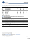
DC Chip Level Specifications
Table 9 lists guaranteed maximum and minimum specifications for the entire voltage and temperature ranges.
Notes
5. Higher storage temperatures reduce data retention time. Recommended storage temperature is +25°C ± 25°C. Extended duration storage temperatures above 85°C
degrade reliability.
6. Human Body Model ESD.
7. According to JESD78 standard.
8. The temperature rise from ambient to junction is package specific. See on page 27. The user must limit the power consumption to comply with this requirement.
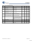
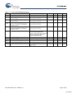
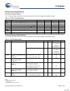
Table 9. DC Chip Level Specifications
Parameter Description Conditions Min Typ Max Units
Vdd Supply Voltage See table titled DC POR and LVD
Specifications on page 20.
1.71 – 3.6 V
I
DD24
Supply Current, IMO = 24 MHz Conditions are Vdd = 3.0V, T
A
= 25
o
C,
CPU = 24 MHz
No I2C/SPI
– – 3.1 mA
I
DD12
Supply Current, IMO = 12 MHz Conditions are Vdd = 3.0V, T
A
= 25
o
C,
CPU = 12 MHz
No I2C/SPI
– – 2.0 mA
I
DD6
Supply Current, IMO = 6 MHz Conditions are Vdd = 3.0V, T
A
= 25
o
C,
CPU = 6 MHz
No I2C/SPI
– – 1.5 mA
I
SB0
Deep Sleep Current Vdd = 3.0V, T
A
= 25
o
C, IO regulator
turned off
– 0.1 – μA
I
SB1
Standby Current with POR, LVD, and
Sleep Timer
Vdd = 3.0V, T
A
= 25
o
C, IO regulator
turned off
– – 1.5 μA
[+] Feedback


