CY7C68033/CY7C68034
Document #: 001-04247 Rev. *D Page 7 of 33
If Autovectoring is enabled (AV4EN = 1 in the INTSET-UP
register), the NX2LP-Flex substitutes its INT4VEC byte.
Therefore, if the high byte (‘page’) of a jump-table address is
preloaded at location 0x554, the automatically-inserted
INT4VEC byte at 0x555 will direct the jump to the correct
address out of the 14 addresses within the page. When the
ISR occurs, the NX2LP-Flex pushes the program counter onto
its stack then jumps to address 0x553, where it expects to find
a ‘jump’ instruction to the ISR Interrupt service routine.
Reset and Wakeup
Reset Pin
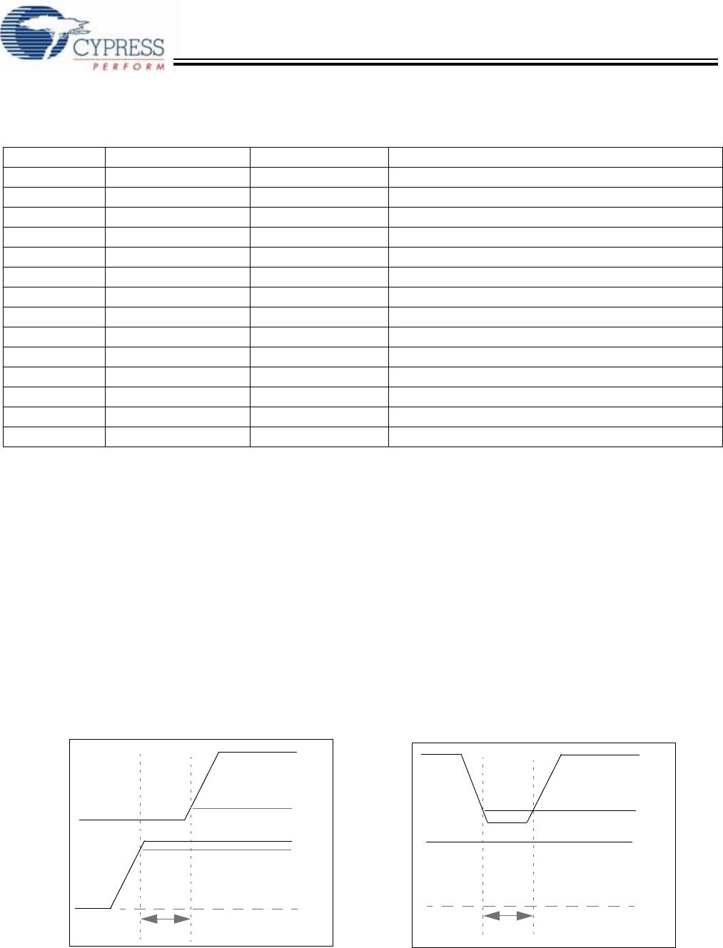
The input pin RESET#, will reset the NX2LP-Flex when
asserted. This pin has hysteresis and is active LOW. When a
crystal is used as the clock source for the NX2LP-Flex, the
reset period must allow for the stabilization of the crystal and
the PLL. This reset period should be approximately 5 ms after
V
CC
has reached 3.0V. If the crystal input pin is driven by a
clock signal, the internal PLL stabilizes in 200 μs after V
CC
has
reached 3.0V
[1]
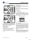
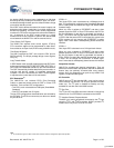
. Figure 5 shows a power-on reset condition
and a reset applied during operation. A power-on reset is
defined as the time reset is asserted while power is being
applied to the circuit. A powered reset is defined to be when
the NX2LP-Flex has previously been powered on and
operating and the RESET# pin is asserted.
Cypress provides an application note which describes and
recommends power on reset implementation and can be found
on the Cypress web site. For more information on reset imple-
mentation for the EZ-USB family of products visit the
http://www.cypress.com website.
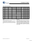
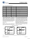
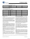
Table 4. Individual FIFO/GPIF Interrupt Sources
Priority INT4VEC Value Source Notes
1 0x580 EP2PF Endpoint 2 Programmable Flag
2 0x584 EP4PF Endpoint 4 Programmable Flag
3 0x588 EP6PF Endpoint 6 Programmable Flag
4 0x58C EP8PF Endpoint 8 Programmable Flag
5 0x590 EP2EF Endpoint 2 Empty Flag
6 0x594 EP4EF Endpoint 4 Empty Flag
7 0x598 EP6EF Endpoint 6 Empty Flag
8 0x59C EP8EF Endpoint 8 Empty Flag
9 0x5A0 EP2FF Endpoint 2 Full Flag
10 0x5A4 EP4FF Endpoint 4 Full Flag
11 0x5A8 EP6FF Endpoint 6 Full Flag
12 0x5AC EP8FF Endpoint 8 Full Flag
13 0x5B0 GPIFDONE GPIF Operation Complete
14 0x5B4 GPIFWF GPIF Waveform
Note
1. If the external clock is powered at the same time as the CY7C68033/CY7C68034 and has a stabilization wait period, it must be added to the 200 μs.
Figure 5. Reset Timing Plots
V
IL
0V
3.3V
3.0V
T
RESET
V
CC
RESET#
Power-on Reset
T
RESET
V
CC
RESET#
V
IL
Powered Reset
3.3V
0V
[+] Feedback


