CY8C22113, CY8C22213
Document Number: 38-12009 Rev. *F Page 29 of 36
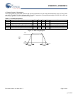
AC External Clock Specifications
The following tables list guaranteed maximum and minimum specifications for the voltage and temperature ranges: 4.75V to 5.25V
and -40
°C ≤ T
A
≤ 85°C, or 3.0V to 3.6V and -40°C ≤ T
A
≤ 85°C, respectively. Typical parameters apply to 5V and 3.3V at 25°C and
are for design guidance only or unless otherwise specified.
AC Programming Specifications
The following table lists guaranteed maximum and minimum specifications for the voltage and temperature ranges: 4.75V to 5.25V
and -40
°C ≤ T
A
≤ 85°C, or 3.0V to 3.6V and -40°C ≤ T
A
≤ 85°C, respectively. Typical parameters apply to 5V and 3.3V at 25°C and
are for design guidance only or unless otherwise specified.
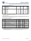
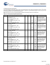
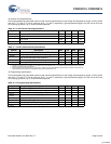
Table 30. 5V AC External Clock Specifications
Symbol Description Min Typ Max Units
F
OSCEXT
Frequency 0 –24.24MHz
– High Period 20.6
– –ns
– Low Period 20.6
– –ns
– Power Up IMO to Switch 150
– – μs
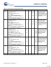
Table 31. 3.3V AC External Clock Specifications
Symbol Description Min Typ Max Units
F
OSCEXT
Frequency with CPU Clock divide by 1
a
0 –12.12MHz
F
OSCEXT
Frequency with CPU Clock divide by 2 or greater
b
0 –24.24MHz
– High Period with CPU Clock divide by 1 41.7
– –ns
– Low Period with CPU Clock divide by 1 41.7
– –ns
– Power Up IMO to Switch 150
– – μs
a. Maximum CPU frequency is 12 MHz at 3.3V. With the CPU clock divider set to 1, the external clock must adhere to the maximum
frequency and duty cycle requirements.
b. If the frequency of the external clock is greater than 12 MHz, the CPU clock divider must be set to 2 or greater. In this case, the
CPU clock divider ensures that the fifty percent duty cycle requirement is met.
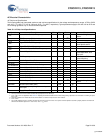
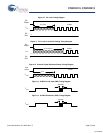
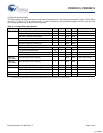
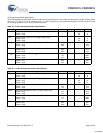
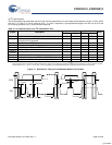
Table 32. AC Programming Specifications
Symbol Description Min Typ Max Units
T
RSCLK
Rise Time of SCLK 1 – 20 ns
T
FSCLK
Fall Time of SCLK 1 – 20 ns
T
SSCLK
Data Setup Time to Falling Edge of SCLK 40 – – ns
T
HSCLK
Data Hold Time from Falling Edge of SCLK 40 – – ns
F
SCLK
Frequency of SCLK 0 – 8 MHz
T
ERASEB
Flash Erase Time (Block) – 15 – ms
T
WRITE
Flash Block Write Time – 30 – ms
T
DSCLK
Data Out Delay from Falling Edge of SCLK – – 45 ns
[+] Feedback


