CY8C24094, CY8C24794
CY8C24894, CY8C24994
Document Number: 38-12018 Rev. *M Page 41 of 47
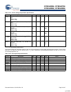
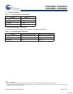
11.1 Thermal Impedance
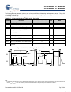
11.2 Solder Reflow Peak Temperature
Following is the minimum solder reflow peak temperature to achieve good solderability.
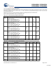
Table 11-1. Thermal Impedance for the Package
Package Typical θ
JA
[15]
56 QFN
[16]
12.93
o
C/W
68 QFN
[16]
13.05
o
C/W
100 VFBGA 65
o
C/W
100 TQFP 51
o
C/W
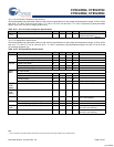
Table 11-2. Solder Reflow Peak Temperature
Package Minimum Peak Temperature
[17]
Maximum Peak Temperature
56 QFN 240
o
C 260
o
C
68 QFN 240
o
C 260
o
C
100 VFBGA 240
o
C 260
o
C
Notes
15.T
J
= T
A
+ POWER x θ
JA
16.To achieve the thermal impedance specified for the QFN package, the center thermal pad should be soldered to the PCB ground plane.
17.Higher temperatures may be required based on the solder melting point. Typical temperatures for solder are 220 ± 5
o
C with Sn-Pb or 245 ± 5
o
C with Sn-Ag-Cu paste.
Refer to the solder manufacturer specifications
[+] Feedback


