


CY8C24123
CY8C24223, CY8C24423
Document Number: 38-12011 Rev. *G Page 21 of 43
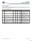
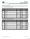
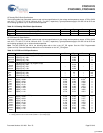
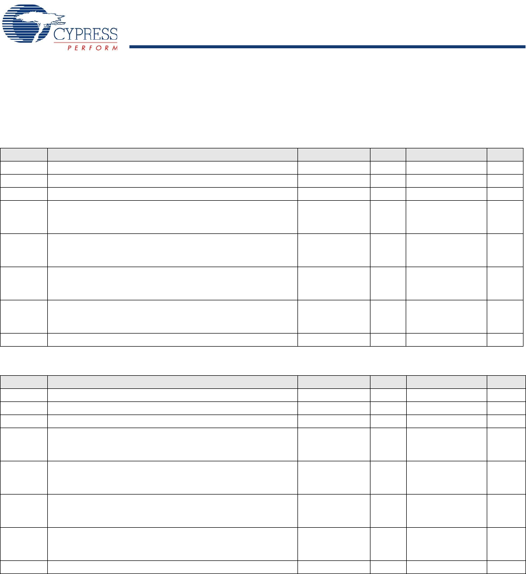
DC Analog Output Buffer Specifications
The following tables list guaranteed maximum and minimum specifications for the voltage and temperature ranges: 4.75V to 5.25V
and -40°C ≤ T
A
≤ 85°C, or 3.0V to 3.6V and -40°C ≤ T
A
≤ 85°C, respectively. Typical parameters apply to 5V and 3.3V at 25°C and
are for design guidance only or unless otherwise specified.
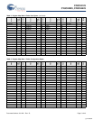
Table 17. 5V DC Analog Output Buffer Specifications
Symbol Description Min Typ Max Units
V
OSOB
Input Offset Voltage (Absolute Value) – 3 12 mV
TCV
OSOB
Average Input Offset Voltage Drift – +6 – μV/°C
V
CMOB
Common-Mode Input Voltage Range 0.5 – Vdd - 1.0 V
R
OUTOB
Output Resistance
Power = Low
Power = High
–
–
1
1
–
–
W
W
V
OHIGHOB
High Output Voltage Swing (Load = 32 ohms to Vdd/2)
Power = Low
Power = High
0.5 x Vdd
+ 1.1
0.5 x Vdd
+ 1.1
–
–
–
–
V
V
V
OLOWOB
Low Output Voltage Swing (Load = 32 ohms to Vdd/2)
Power = Low
Power = High
–
–
–
–
0.5 x Vdd
- 1.3
0.5 x Vdd
- 1.3
V
V
I
SOB
Supply Current Including Bias Cell (No Load)
Power = Low
Power = High
–
–
1.1
2.6
5.1
8.8
mA
mA
PSRR
OB
Supply Voltage Rejection Ratio 60 – – dB
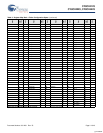
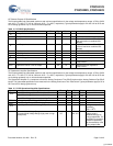
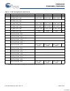
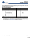
Table 18. 3.3V DC Analog Output Buffer Specifications
Symbol Description Min Typ Max Units
V
OSOB
Input Offset Voltage (Absolute Value) – 3 12 mV
TCV
OSOB
Average Input Offset Voltage Drift – +6 – μV/°C
V
CMOB
Common-Mode Input Voltage Range 0.5 - Vdd - 1.0 V
R
OUTOB
Output Resistance
Power = Low
Power = High
–
–
1
1
–
–
W
W
V
OHIGHOB
High Output Voltage Swing (Load = 1K ohms to Vdd/2)
Power = Low
Power = High
0.5 x Vdd
+ 1.0
0.5 x Vdd
+ 1.0
–
–
–
–
V
V
V
OLOWOB
Low Output Voltage Swing (Load = 1K ohms to Vdd/2)
Power = Low
Power = High
–
–
–
–
0.5 x Vdd
- 1.0
0.5 x Vdd
- 1.0
V
V
I
SOB
Supply Current Including Bias Cell (No Load)
Power = Low
Power = High –
0.8
2.0
2.0
4.3
mA
mA
PSRR
OB
Supply Voltage Rejection Ratio 50 – – dB
[+] Feedback