


CY8C24123
CY8C24223, CY8C24423
Document Number: 38-12011 Rev. *G Page 24 of 43
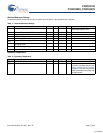
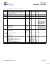
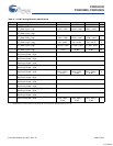
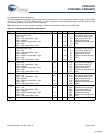
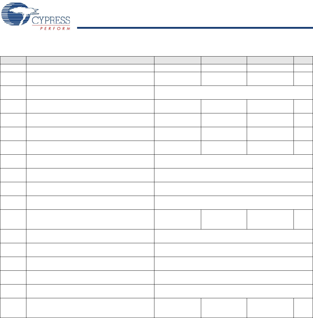
Table 21. 3.3V DC Analog Reference Specifications
Symbol Description Min Typ Max Units
BG Bandgap Voltage Reference 1.274 1.30 1.326 V
– AGND = Vdd/2
a
CT Block Power = High Vdd/2 - 0.037 Vdd/2 - 0.020 Vdd/2 + 0.002 V
– AGND = 2 x BandGap
a
CT Block Power = High
Not Allowed
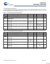
– AGND = P2[4] (P2[4] = Vdd/2)
CT Block Power = High
P2[4] - 0.008 P2[4] + 0.001 P2[4] + 0.009 V
– AGND = BandGap
a
CT Block Power = High BG - 0.009 BG + 0.005 BG + 0.015 V
– AGND = 1.6 x BandGap
a
CT Block Power = High 1.6 x BG - 0.027 1.6 x BG - 0.010 1.6 x BG + 0.018 V
– AGND Column to Column Variation (AGND = Vdd/2)
a
CT Block Power = High -0.034 0.000 0.034 mV
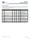
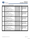
– RefHi = Vdd/2 + BandGap
Ref Control Power = High
Not Allowed
– RefHi = 3 x BandGap
Ref Control Power = High
Not Allowed
– RefHi = 2 x BandGap + P2[6] (P2[6] = 0.5V)
Ref Control Power = High
Not Allowed
– RefHi = P2[4] + BandGap (P2[4] = Vdd/2)
Ref Control Power = High
Not Allowed
– RefHi = P2[4] + P2[6] (P2[4] = Vdd/2, P2[6] = 0.5V)
Ref Control Power = High
P2[4] + P2[6] -
0.075
P2[4] + P2[6] -
0.009
P2[4] + P2[6] +
0.057
V
– RefHi = 3.2 x BandGap
Ref Control Power = High
Not Allowed
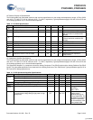
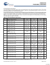
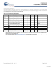
– RefLo = Vdd/2 - BandGap
Ref Control Power = High
Not Allowed
– RefLo = BandGap
Ref Control Power = High
Not Allowed
– RefLo = 2 x BandGap - P2[6] (P2[6] = 0.5V)
Ref Control Power = High
Not Allowed
– RefLo = P2[4] – BandGap (P2[4] = Vdd/2)
Ref Control Power = High
Not Allowed
– RefLo = P2[4]-P2[6] (P2[4] = Vdd/2, P2[6] = 0.5V)
Ref Control Power = High
P2[4] - P2[6] -
0.048
P2[4]- P2[6] +
0.022
P2[4] - P2[6] +
0.092
V
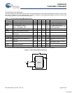
a. AGND tolerance includes the offsets of the local buffer in the PSoC block. Bandgap voltage is 1.3V ± 2%
[+] Feedback