


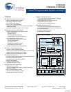
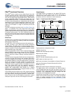
CY8C24123
CY8C24223, CY8C24423
Document Number: 38-12011 Rev. *G Page 9 of 43
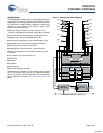
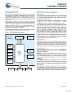
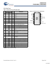
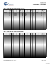
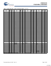
28-Pin Part Pinout
Table 5. 28-Pin Part Pinout (PDIP, SSOP, SOIC)
Pin
No.
Type
Pin
Name
Description
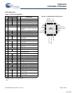
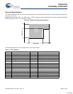
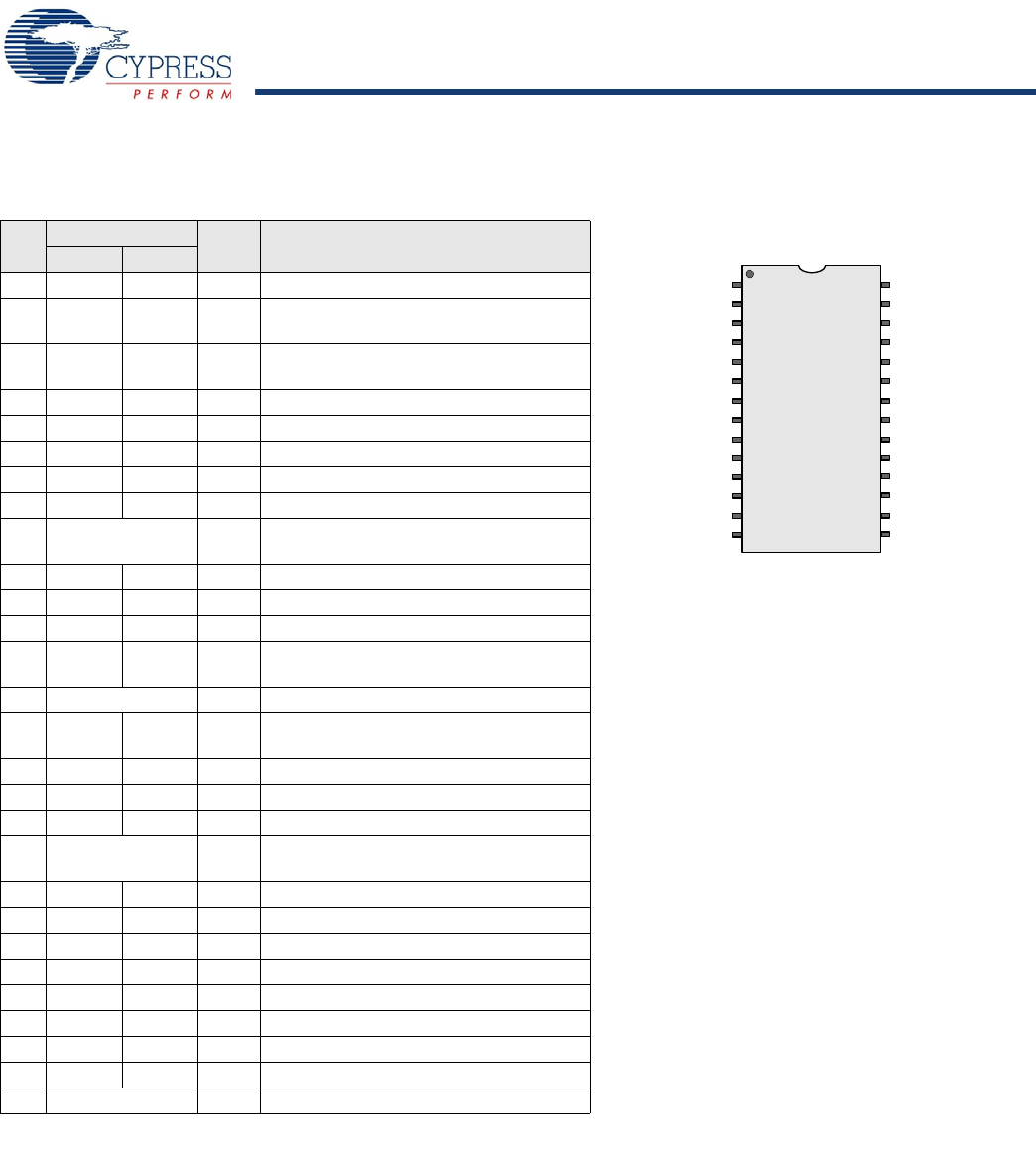
Figure 8. CY8C24423 28-Pin PSoC Device
Digital Analog
1 IO I P0[7] Analog column mux input
2 IO IO P0[5] Analog column mux input and column
output
3 IO IO P0[3] Analog column mux input and column
output
4 IO I P0[1] Analog column mux input.
5 IO P2[7]
6 IO P2[5]
7 IO I P2[3] Direct switched capacitor block input
8 IO I P2[1] Direct switched capacitor block input
9 Power SMP Switch Mode Pump (SMP) connection to
external components required
10 IO P1[7] I2C Serial Clock (SCL)
11 IO P1[5] I2C Serial Data (SDA)
12 IO P1[3]
13 IO P1[1] Crystal Input (XTALin), I2C Serial Clock
(SCL)
14 Power Vss Ground connection
15 IO P1[0] Crystal Output (XTALout), I2C Serial
Data (SDA)
16 IO P1[2]
17 IO P1[4] Optional External Clock Input (EXTCLK)
18 IO P1[6]
19 Input XRES Active high external reset with internal
pull down
20 IO I P2[0] Direct switched capacitor block input
21 IO I P2[2] Direct switched capacitor block input
22 IO P2[4] External Analog Ground (AGND)
23 IO P2[6] External Voltage Reference (VRef)
24 IO I P0[0] Analog column mux input
25 IO I P0[2] Analog column mux input
26 IO I P0[4] Analog column mux input
27 IO I P0[6] Analog column mux input
28 Power Vdd Supply voltage
LEGEND: A = Analog, I = Input, and O = Output.
AI, P0[7]
AIO, P0[5]
AIO, P0[3]
AI, P0[1]
P2[7]
P2[5]
AI, P2[3]
AI, P2[1]
SMP
I2C SCL, P1[7]
I2C SDA, P1[5]
P1[3]
I2C SCL, XTALin, P1[1]
Vss
Vdd
P0[6], AI
P0[4], AI
P0[2], AI
P0[0], AI
P2[6], External VRef
P2[4], External AGND
P2[2], AI
P2[0], AI
XRES
P1[6]
P1[4], EXTCLK
P1[2]
P1[0], XTALout, I2C SDA
PDIP
SSOP
SOIC
1
2
3
4
5
6
7
8
9
10
11
12
13
14
28
27
26
25
24
23
22
21
20
19
18
17
16
15
[+] Feedback