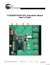
CYS25G0101DX-ATC Evaluation Board User’s Guide
8
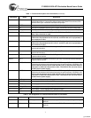
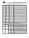
5 RXD13 HSTL output Parallel receive data output RXD13. The outputs change following
RXCLK↓
7 RXD12 HSTL output Parallel receive data output RXD12. The outputs change following
RXCLK↓
9 RXD11 HSTL output Parallel receive data output RXD11. The outputs change following
RXCLK↓
11 RXD10 HSTL output Parallel receive data output RXD10. The outputs change following
RXCLK↓
13 RXD9 HSTL output Parallel receive data output RXD9. The outputs change following RX-
CLK↓
15 RXD8 HSTL output Parallel receive data output RXD8. The outputs change following RX-
CLK↓
17 RXD7 HSTL output Parallel receive data output RXD7. The outputs change following RX-
CLK↓
19 RXD6 HSTL output Parallel receive data output RXD6. The outputs change following RX-
CLK↓
21 RXD5 HSTL output Parallel receive data output RXD5. The outputs change following RX-
CLK↓
23 RXD4 HSTL output Parallel receive data output RXD4. The outputs change following RX-
CLK↓
25 RXD3 HSTL output Parallel receive data output RXD3. The outputs change following RX-
CLK↓
27 RXD2 HSTL output Parallel receive data output RXD2. The outputs change following RX-
CLK↓
29 RXD1 HSTL output Parallel receive data output RXD1. The outputs change following RX-
CLK↓
31 RXD0 HSTL output Parallel receive data output RXD0. The outputs change following RX-
CLK↓
2, 4, 6, 8, 10,
12, 14, 16, 18,
20, 22, 24, 26,
28, 30, 32
GND Ground Ground
J10 RXCLK HSTL output Receive clock output. This clock is divided by 16 of the bit-rate clock
extracted from the received serial stream
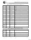
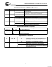
Table 3. Pin Assignment of J2 Header and Description of J9 Header
Pin Number Name I/O Characteristics Description
1, 3, 5, 7, 9, 11,
13, 15, 17, 19,
21, 23, 25, 27,
29, 31
GND Ground Ground
2 TXD15 HSTL output Parallel transmit data input TXD15. The input data is sampled by TX-
CLKI↑
4 TXD14 HSTL input Parallel transmit data input TXD14. The input data is sampled by TX-
CLKI↑
6 TXD13 HSTL input Parallel transmit data input TXD13. The input data is sampled by TX-
CLKI↑
Table 2. Pin Assignment of J1 Header and Description of J10 Header (continued)
Pin Number Name I/O Characteristics Description
[+] Feedback


