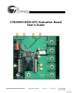
CYS25G0101DX-ATC Evaluation Board User’s Guide
9
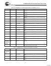
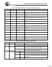
8 TXD12 HSTL input Parallel transmit data input TXD12. The input data is sampled by TX-
CLKI↑
10 TXD11 HSTL input Parallel transmit data input TXD10. The input data is sampled by TX-
CLKI↑
12 TXD10 HSTL input Parallel transmit data input TXD9. The input data is sampled by TX-
CLKI↑
14 TXD9 HSTL input Parallel transmit data input TXD8. The input data is sampled by TX-
CLKI↑
16 TXD8 HSTL input Parallel transmit data input TXD8. The input data is sampled by TX-
CLKI↑
18 TXD7 HSTL input Parallel transmit data input TXD7. The input data is sampled by TX-
CLKI↑
20 TXD6 HSTL input Parallel transmit data input TXD6. The input data is sampled by TX-
CLKI↑
22 TXD5 HSTL input Parallel transmit data ‘input TXD5. The input data is sampled by TX-
CLKI↑
24 TXD4 HSTL input Parallel transmit data input TXD4. The input data is sampled by TX-
CLKI↑
26 TXD3 HSTL input Parallel transmit data input TXD3. The input data is sampled by TX-
CLKI↑
28 TXD2 HSTL input Parallel transmit data input TXD2. The input data is sampled by TX-
CLKI↑
30 TXD1 HSTL input Parallel transmit data input TXD1. The input data is sampled by TX-
CLKI↑
32 TXD0 HSTL input Parallel transmit data input TXD0. The input data is sampled by TX-
CLKI↑
J9 TXCLKI HSTL input Parallel transmit data input clock
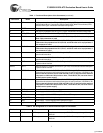
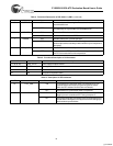
Table 4. Functional Description of DIP Switch 1 (SW1)
Position Name State Description
1 RESET ON* Disable Reset - Normal operation
OFF Reset for all logic functions except the transmit FIFO
2 DIAGLOOP ON Transmit data (from TXD[15:0]) is routed through the receive clock
and data recovery and presented at RXD[15:0] output
OFF* Received serial data (from IN±) is routed through the receive clock and
data recovery and presented at RXD[15:0] output
3, 4 LINELOOP,
LOOPA
ON ON Invalid setting
ON OFF Received serial data is looped back from receive input (IN±) to trans-
mit output (OUT±) after being reclocked by the recovered clock
OFF ON Received serial data is looped back from receive input (IN±) to trans-
mit output (OUT±), but is not routed through the clock and data
recovery PLL
OFF* OFF* Disable serial data loop back.
Table 3. Pin Assignment of J2 Header and Description of J9 Header (continued)
Pin Number Name I/O Characteristics Description
[+] Feedback


