


STK14C88-5
Document Number: 001-51038 Rev. ** Page 10 of 17
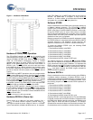
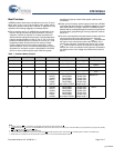
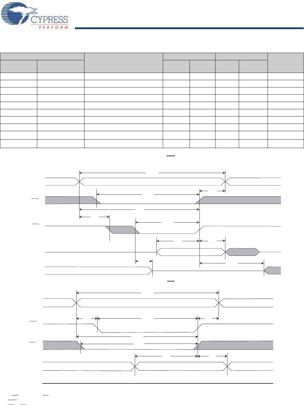
SRAM Write Cycle
Parameter
Description
35 ns 45 ns
Unit
Min Max Min Max
Cypress
Parameter
Alt
t
WC
t
AVAV
Write Cycle Time 35 45 ns
t
PWE
t
WLWH,
t
WLEH
Write Pulse Width 25 30 ns
t
SCE
t
ELWH,
t
ELEH
Chip Enable To End of Write 25 30 ns
t
SD
t
DVWH,
t
DVEH
Data Setup to End of Write 12 15 ns
t
HD
t
WHDX,
t
EHDX
Data Hold After End of Write 0 0 ns
t
AW
t
AVWH,
t
AVEH
Address Setup to End of Write 25 30 ns
t
SA
t
AVWL,
t
AVEL
Address Setup to Start of Write 0 0 ns
t
HA
t
WHAX,
t
EHAX
Address Hold After End of Write 0 0 ns
t
HZWE
[11,12]
t
WLQZ
Write Enable to Output Disable 13 15 ns
t
LZWE
[11]
t
WHQX
Output Active After End of Write 5 5 ns
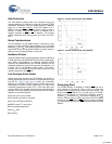
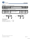
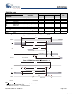
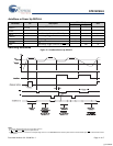
Switching Waveforms
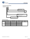
Figure 10. SRAM Write Cycle 1: WE Controlled
[13, 14]
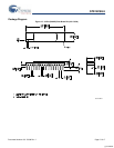
Figure 11. SRAM Write Cycle 2: CE Controlled
[13, 14]
t
WC
t
SCE
t
HA
t
AW
t
SA
t
PWE
t
SD
t
HD
t
HZWE
t
LZWE
ADDRESS
CE
WE
DATA IN
DATA OUT
DATA VALID
HIGH IMPEDANCE
PREVIOUS DATA
t
WC
ADDRESS
t
SA
t
SCE
t
HA
t
AW
t
PWE
t
SD
t
HD
CE
WE
DATA IN
DATA OUT
HIGH IMPEDANCE
DATA VALID
Notes
12.If WE
is Low when CE goes Low, the outputs remain in the high impedance state.
13.HSB
must be high during SRAM WRITE cycles.
14.
CE
or WE must be greater than V
IH
during address transitions.
[+] Feedback