


STK14C88-5
Document Number: 001-51038 Rev. ** Page 2 of 17
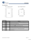
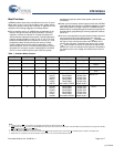
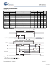
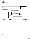
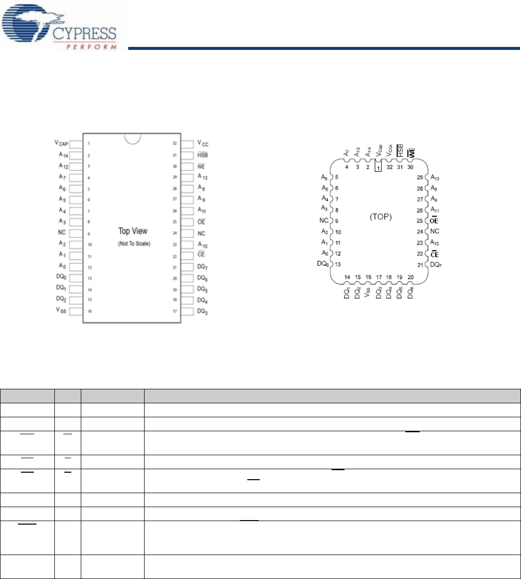
Pin Configurations
Pin Definitions
Pin Name Alt IO Type Description
A
0
–A
14
Input Address Inputs. Used to select one of the 32,768 bytes of the nvSRAM.
DQ
0
-DQ
7
Input or Output Bidirectional Data IO Lines. Used as input or output lines depending on operation.
WE
W
Input Write Enable Input, Active LOW. When the chip is enabled and WE is LOW, data on the IO
pins is written to the specific address location.
CE
E
Input Chip Enable Input, Active LOW. When LOW, selects the chip. When HIGH, deselects the chip.
OE
G
Input Output Enable, Active LOW. The active LOW OE input enables the data output buffers during
read cycles. Deasserting OE
HIGH causes the IO pins to tri-state.
V
SS
Ground Ground for the Device. The device is connected to ground of the system.
V
CC
Power Supply Power Supply Inputs to the Device.
HSB
Input or Output Hardware Store Busy (HSB). When LOW, this output indicates a Hardware Store is in progress.
When pulled low external to the chip, it initiates a nonvolatile STORE operation. A weak internal
pull up resistor keeps this pin high if not connected (connection optional).
V
CAP
Power Supply AutoStore
Capacitor. Supplies power to nvSRAM during power loss to store data from SRAM
to nonvolatile elements.
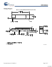
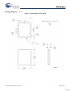
Figure 1. Pin Diagram: 32-Pin DIP
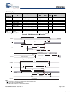
Figure 2. Pin Diagram: 32-Pin LCC
[+] Feedback