


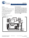
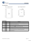
STK14C88-5
Document Number: 001-51038 Rev. ** Page 7 of 17
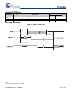
Maximum Ratings
Exceeding maximum ratings may shorten the useful life of the
device. These user guidelines are not tested.
Storage Temperature ................................. –65°C to +150°C
Temperature under Bias ............................. –55°C to +125°C
Voltage on Input Relative to GND.....................–0.5V to 7.0V
Voltage on Input Relative to Vss............–0.6V to V
CC
+ 0.5V
Voltage on DQ
0-7
or HSB .......................–0.5V to Vcc + 0.5V
Power Dissipation.......................................................... 1.0W
DC output Current (1 output at a time, 1s duration) ....15 mA
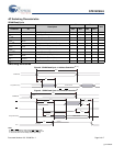
Operating Range
Range Ambient Temperature V
CC
Military -55°C to +125°C 4.5V to 5.5V
DC Electrical Characteristics
Over the operating range (V
CC
= 4.5V to 5.5V)
[6]
Parameter Description Test Conditions Min Max Unit
I
CC1
Average V
CC
Current t
RC
= 35 ns
t
RC
= 45 ns
Dependent on output loading and cycle rate. Values obtained
without output loads.
I
OUT
= 0 mA.
85
70
mA
mA
I
CC2
Average V
CC
Current
during STORE
All Inputs Do Not Care, V
CC
= Max
Average current for duration t
STORE
3mA
I
CC3
Average V
CC
Current at
t
RC
= 200 ns, 5V, 25°C
Typical
WE
> (V
CC
– 0.2V). All other inputs cycling.
Dependent on output loading and cycle rate. Values obtained
without output loads.
10 mA
I
CC4
Average V
CAP
Current
during AutoStore Cycle
All Inputs Do Not Care, V
CC
= Max
Average current for duration t
STORE
2mA
I
SB1
[7]
V
CC
Standby Current
(Standby, Cycling TTL
Input Levels)
t
RC
= 35 ns, CE > V
IH
t
RC
= 45 ns, CE > V
IH
26
23
mA
mA
I
SB2
[7]
V
CC
Standby Current CE > (V
CC
– 0.2V). All others V
IN
< 0.2V or > (V
CC
– 0.2V).
Standby current level after nonvolatile cycle is complete.
Inputs are static. f = 0 MHz.
1.5 mA
I
IX
Input Leakage Current V
CC
= Max, V
SS
< V
IN
< V
CC
-1 +1 μA
I
OZ
Off State Output Leakage
Current
V
CC
= Max, V
SS
< V
IN
< V
CC
, CE or OE > V
IH
or WE < V
IL
-5 +5 μA
V
IH
Input HIGH Voltage 2.2 V
CC
+
0.5
V
V
IL
Input LOW Voltage V
SS
–
0.5
0.8 V
V
OH
Output HIGH Voltage I
OUT
= –4 mA 2.4 V
V
OL
Output LOW Voltage I
OUT
= 8 mA 0.4 V
V
BL
Logic ‘0’ Voltage on HSB
Output
I
OUT
= 3 mA 0.4 V
V
CAP
Storage Capacitor Between V
CAP
pin and Vss, 6V rated. 68 µF +20% nom. 54 260 uF
Data Retention and Endurance
Parameter Description Min Unit
DATA
R
Data Retention 100 Years
NV
C
Nonvolatile STORE Operations 1,000 K
Notes
6. V
CC
reference levels throughout this data sheet refer to V
CC
if that is where the power supply connection is made, or V
CAP
if V
CC
is connected to ground.
7. CE
> V
IH
does not produce standby current levels until any nonvolatile cycle in progress has timed out.
[+] Feedback