


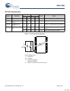
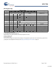

STK17T88
Document Number: 001-52040 Rev. *A Page 13 of 22
Software STORE
Data can be transferred from the SRAM to the nonvolatile
memory by a software address sequence. The STK17T88
software
STORE cycle is initiated by executing sequential E
controlled READ cycles from six specific address locations in
exact order. During the
STORE cycle, previous data is erased
and then the new data is programmed into the nonvolatile
elements. Once a
STORE cycle is initiated, further memory
inputs and outputs are disabled until the cycle is completed.
To initiate the software
STORE cycle, the following READ
sequence must be performed:
1. Read address 0x0E38, Valid READ
2. Read address 0x31C7, Valid READ
3. Read address 0x03E0, Valid READ
4. Read address 0x3C1F, Valid READ
5. Read address 0x303F, Valid READ
6. Read address 0x0FC0, Initiate STORE cycle
Once the sixth address in the sequence has been entered, the
STORE cycle commences and the chip is disabled. It is
important that READ cycles and not WRITE cycles be used in
the sequence. After the t
STORE
cycle time has been fulfilled, the
SRAM is again activated for READ and WRITE operation.
Software RECALL
Data can be transferred from the nonvolatile memory to the
SRAM by a software address sequence. A software
RECALL
cycle is initiated with a sequence of READ operations in a man-
ner similar to the software
STORE initiation. To initiate the
RECALL cycle, the following sequence of E controlled READ
operations must be performed:
1. Read address 0x0E38, Valid READ
2. Read address 0x31C7, Valid READ
3. Read address 0x03E0, Valid READ
4. Read address 0x3C1F, Valid READ
5. Read address 0x303F, Valid READ
6. Read address 0x0C63, Initiate RECALL cycle
Internally,
RECALL is a two-step procedure. First, the SRAM
data is cleared, and second, the nonvolatile information is trans-
ferred into the SRAM cells. After the t
RECALL
cycle time, the
SRAM is again ready for READ or WRITE operations. The
RECALL operation in no way alters the data in the nonvolatile
storage elements.
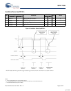
Data Protection
The STK17T88 protects data from corruption during low-voltage
conditions by inhibiting all externally initiated STORE and
WRITE operations. The low-voltage condition is detected when
V
CC
<V
SWITCH
.
If the STK17T88 is in a WRITE mode (both E
and W low) at
power up, after a
RECALL, or after a STORE, the WRITE is
inhibited until a negative transition on E
or W is detected. This
protects against inadvertent writes during power up or brown out
conditions.
Noise Considerations
The STK17T88 is a high-speed memory and so must have a
high-frequency bypass capacitor of 0.1 µF connected between
both V
CC
pins and V
SS
ground plane with no plane break to chip
V
SS
. Use leads and traces that are as short as possible. As with
all high-speed CMOS ICs, careful routing of power, ground, and
signals reduce circuit noise.
Preventing AutoStore
Because of the use of nvSRAM to store critical RTC data, the
AutoStore function can not be disabled on the STK17T88.
Best Practices
nvSRAM products have been used effectively for over 15 years.
While ease-of-use is one of the product’s main system values,
experience gained working with hundreds of applications has
resulted in the following suggestions as best practices:
■ The nonvolatile cells in an nvSRAM are programmed on the
test floor during final test and quality assurance. Incoming
inspection routines at customer or contract manufacturer’s
sites sometimes reprograms these values. Final NV patterns
are typically repeating patterns of AA, 55, 00, FF, A5, or 5A.
End product’s firmware should not assume an NV array is in a
set programmed state. Routines that check memory content
values to determine first time system configuration, cold or
warm boot status, etc. should always program a unique NV
pattern (e.g., complex 4-byte pattern of 46 E6 49 53 hex or
more random bytes) as part of the final system manufacturing
test to ensure these system routines work consistently.
■ Power up boot firmware routines should rewrite the nvSRAM
into the desired state (autostore enabled, etc.). While the
nvSRAM is shipped in a preset state, best practice is to again
rewrite the nvSRAM into the desired state as a safeguard
against events that might flip the bit inadvertently (program
bugs, incoming inspection routines, etc.).
■ The OSCEN bit in the Calibration register at 0x7FF8 should be
set to 1 to preserve battery life when the system is in storage
(see Stopping and Starting the RTC Oscillator on page 14.
■ The V
CAP
value specified in this datasheet includes a minimum
and a maximum value size. Best practice is to meet this
requirement and not exceed the max V
CAP
value because the
nvSRAM internal algorithm calculates V
CAP
charge time based
on this max Vcap value. Customers that want to use a larger
V
CAP
value to make sure there is extra store charge and store
time should discuss their V
cap
size selection with Cypress to
understand any impact on the V
CAP
voltage level at the end of
a t
RECALL
period.
[+] Feedback