


STK17T88
Document Number: 001-52040 Rev. *A Page 6 of 22
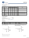
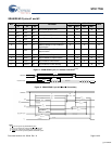
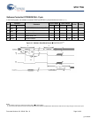
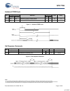
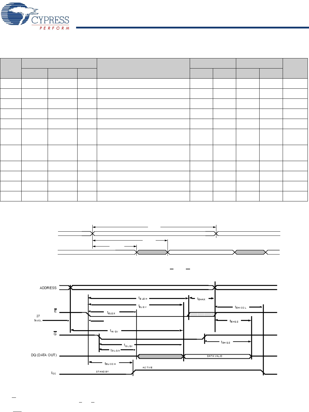
SRAM READ Cycles #1 and #2
Figure 5. SRAM READ Cycle #1: Address Controlled
[3,4,6]
Figure 6. SRAM READ Cycle #2: E and G Controlled
[6]
Notes
3. W
must be high during SRAM READ cycles.
4. Device is continuously selected with E
and G both low
5. Measured ± 200mV from steady state output voltage.
6. HSB
must remain high during READ and WRITE cycles.
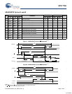
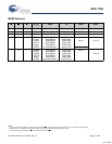
NO.
Symbols
Parameter
STK17T88-25 STK17T88-45
Units
#1 #2 Alt. Min Max Min Max
1t
ELQV
t
ACS
Chip Enable Access Time 25 45 ns
2t
AVAV
[3]
t
ELEH
[5]
t
RC
Read Cycle Time 25 45 ns
3t
AVQV
[4]
t
AVQV
[6]
t
AA
Address Access Time 25 45 ns
4t
GLQV
t
OE
Output Enable to Data Valid 12 20 ns
5t
AXQX
[4]
t
AXQX
t
OH
Output Hold after Address Change 3 3 ns
6t
ELQX
t
LZ
Address Change or Chip Enable to
Output Active
33ns
7t
EHQZ
t
HZ
Address Change or Chip Disable to
Output Inactive
10 15 ns
8t
GLQX
t
OLZ
Output Enable to Output Active 0 0 ns
9t
GHQZ
[5]
t
OHZ
Output Disable to Output Inactive 10 15 ns
10 t
ELICCL
[3]
t
PA
Chip Enable to Power Active 0 0 ns
11 t
EHICCH
[3]
t
PS
Chip Disable to Power Standby 25 45 ns
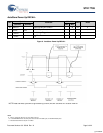
DATA VALID
5
t
AXQX
3
t
AVQV
DQ (DATA OUT)
ADDRESS
2
t
AVAV
2
29
11
7
9
10
8
4
3
6
1
[+] Feedback