


STK17T88
Document Number: 001-52040 Rev. *A Page 3 of 22
Absolute Maximum Ratings
Voltage on Input Relative to Ground.................–0.5V to 4.1V
Voltage on Input Relative to V
SS
...........–0.5V to (V
CC
+ 0.5V)
Voltage on DQ
0-7
or HSB......................–0.5V to (V
CC
+ 0.5V)
Temperature under Bias ............................... –55°C to 125°C
Junction Temperature................................... –55°C to 140°C
Storage Temperature.................................... –65°C to 150°C
Power Dissipation.............................................................1W
DC Output Current (1 output at a time, 1s duration).... 15 mA
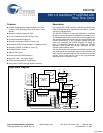
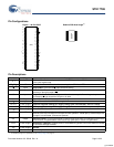
RF (SSOP-48) Package Thermal Characteristics
θ
jc
6.2 C/W; θ
ja
51.1 [0fpm], 44.7 [200fpm], 41.8 C/W [500fpm]
Note: Stresses greater than those listed under “Absolute
Maximum Ratings” may cause permanent damage to the device.
This is a stress rating only, and functional operation of the device
at conditions above those indicated in the operational sections
of this specification is not implied. Exposure to absolute
maximum rating conditions for extended periods may affect
reliability.
Note:The HSB
pin has I
OUT
=-10uA for V
OH
of 2.4V, this parameter is characterized but not tested.
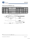
Note:The INT is open-drain and does not source or sink high current when interrupt Register bit D3 is below.
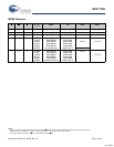
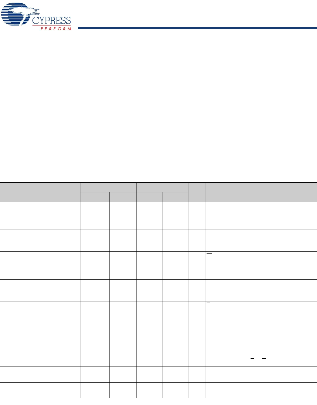
DC Characteristics
(V
CC
= 2.7V-3.6V)
Symbol Parameter
Commercial Industrial
Units Notes
Min Max Min Max
I
CC
1
Average V
CC
Current 65
50
70
55
mA
mA
t
AVAV
= 25 ns
t
AVAV
= 45 ns
Dependent on output loading and cycle rate.
Values obtained without output loads.
I
CC
2
Average V
CC
Current
during STORE
3 3 mA All Inputs Don’t Care, V
CC
= max
Average current for duration of STORE
cycle (t
STORE
)
I
CC
3
Average V
CC
Current
at t
AVAV
= 200ns
3V, 25°C, Typical
10 10 mA W
≥ (V
CC
– 0.2V)
All Other Inputs Cycling at CMOS Levels
Dependent on output loading and cycle rate.
Values obtained without output loads.
I
CC
4
Average V
CAP
Current during
AutoStore™ Cycle
3 3 mA All Inputs Don’t Care
Average current for duration of STORE cycle
(t
STORE
)
I
SB
V
CC
Standby Current
(Standby, Stable
CMOS Levels)
33mAE
≥ (V
CC
-0.2V)
All Others V
IN
≤ 0.2V or ≥ (V
CC
-0.2V)
Standby current level after nonvolatile cycle
complete
I
ILK
Input Leakage
Current
±1 ±1 µAV
CC
= max
V
IN
= V
SS
to V
CC
I
OLK
Off-State Output
Leakage Current
±1 ±1 µAV
CC
= max
V
IN
= V
SS
to V
CC
, E or G ≥ V
IH
V
IH
Input Logic “1”
Voltage
2.0 V
CC
+ 0.5 2.0 V
CC
+ 0.5 V All Inputs
V
IL
Input Logic “0”
Voltage
V
SS
–0.5 0.8 V
SS
–0.5 0.8 V All Inputs
[+] Feedback