


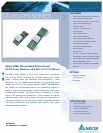

DS_DNM04SIP10_07162008D
8
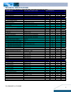
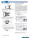
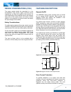
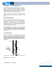
TEST CONFIGURATIONS
V
I
(+)
V
I
(-)
BATTERY
2
100uF
Tantalum
L
TO OSCILLOSCOPE
Note: Input reflected-ripple current is measured with a
simulated source inductance. Current is measured at
the input of the module.
Figure 29: Input reflected-ripple test setup
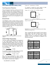
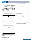
Vo
GND
COPPER STRIP
10uF
tantalum
1uF
ceramic
SCOPE
Resistive
Load
Note: Use a 10μF tantalum and 1μF capacitor. Scope
measurement should be made using a BNC cable.
Figure 30: Peak-peak output noise and startup transient
measurement test setup.
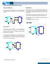
SUPPLY
I
I
V
I
Vo
GND
Io
LOAD
CONTACT AND
DISTRIBUTION LOSSES
CONTACT RESISTANCE
Vo
Vin
Figure 31: Output voltage and efficiency measurement test
setup
Note: All measurements are taken at the module
terminals. When the module is not soldered (via
socket), place Kelvin connections at module
terminals to avoid measurement errors due to
contact resistance.
%100)( ×
×
×
=
IiVi
IoVo
η
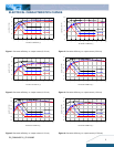
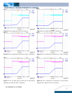
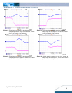
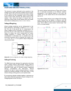
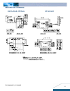
DESIGN CONSIDERATIONS
Input Source Impedance
To maintain low noise and ripple at the input voltage, it is
critical to use low ESR capacitors at the input to the
module. Figure 32 shows the input ripple voltage (mVp-p)
for various output models using 200 µF(2 x100uF) low
ESR
tantalum capacitor (KEMET p/n: T491D107M016AS,
AVX p/n: TAJD107M106R, or equivalent) in parallel with
47 µF ceramic capacitor (TDK p/n:C5750X7R1C476M or
equivalent). Figure 33 shows much lower input voltage
ripple when input capacitance is increased to 400 µF (4 x
100 µF)
tantalum capacitors in parallel with 94 µF (2 x 47
µF) ceramic capacitor.
The input capacitance should be able to handle an AC
ripple current of at least:
Arms
Vin
Vout
Vin
Vout
IoutIrms
⎟
⎠
⎞
⎜
⎝
⎛
−= 1
0
50
100
150
200
250
300
350
01234
Output Voltage (Vdc)
Input Ripple Voltage (mVp-p)
5.0Vin
3.3Vin
Figure 32: Input voltage ripple for various output models, IO =
10 A (CIN = 2
×
100 µF tantalum // 47 µF ceramic)
0
50
100
150
200
01234
Output Voltage (Vdc)
Input Ripple Voltage (mVp-p)
5.0Vin
3.3Vin
Figure 33: Input voltage ripple for various output models, IO =
10 A (CIN = 4
×
100 µF tantalum // 2
×
47 µF ceramic)