


1
June 1998
82C55A
CMOS Programmable
Peripheral Interface
Features
• Pin Compatible with NMOS 8255A
• 24 Programmable I/O Pins
• Fully TTL Compatible
• High Speed, No “Wait State” Operation with 5MHz and
8MHz 80C86 and 80C88
• Direct Bit Set/Reset Capability
• Enhanced Control Word Read Capability
• L7 Process
• 2.5mA Drive Capability on All I/O Ports
• Low Standby Power (ICCSB) . . . . . . . . . . . . . . . . .10µA
Description
The Intersil 82C55A is a high performance CMOS version of
the industry standard 8255A and is manufactured using a
self-aligned silicon gate CMOS process (Scaled SAJI IV). It
is a general purpose programmable I/O device which may be
used with many different microprocessors. There are 24 I/O
pins which may be individually programmed in 2 groups of
12 and used in 3 major modes of operation. The high
performance and industry standard configuration of the
82C55A make it compatible with the 80C86, 80C88 and
other microprocessors.
Static CMOS circuit design insures low operating power. TTL
compatibility over the full military temperature range and bus
hold circuitry eliminate the need for pull-up resistors. The
Intersil advanced SAJI process results in performance equal
to or greater than existing functionally equivalent products at
a fraction of the power.
Ordering Information
PART NUMBERS
PACKAGE
TEMPERATURE
RANGE
PKG.
NO.5MHz 8MHz
CP82C55A-5 CP82C55A
40 Ld PDIP
0
o
C to 70
o
C E40.6
IP82C55A-5 IP82C55A -40
o
C to 85
o
C E40.6
CS82C55A-5 CS82C55A
44 Ld PLCC
0
o
C to 70
o
C N44.65
IS82C55A-5 IS82C55A -40
o
C to 85
o
C N44.65
CD82C55A-5 CD82C55A
40 Ld
CERDIP
0
o
C to 70
o
C F40.6
ID82C55A-5 ID82C55A -40
o
C to 85
o
C F40.6
MD82C55A-5/B MD82C55A/B -55
o
C to 125
o
C F40.6
8406601QA 8406602QA SMD# F40.6
MR82C55A-5/B MR82C55A/B
44 Pad
CLCC
-55
o
C to 125
o
C J44.A
8406601XA 8406602XA SMD# J44.A
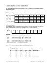
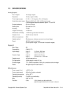
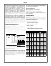
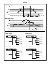
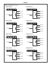
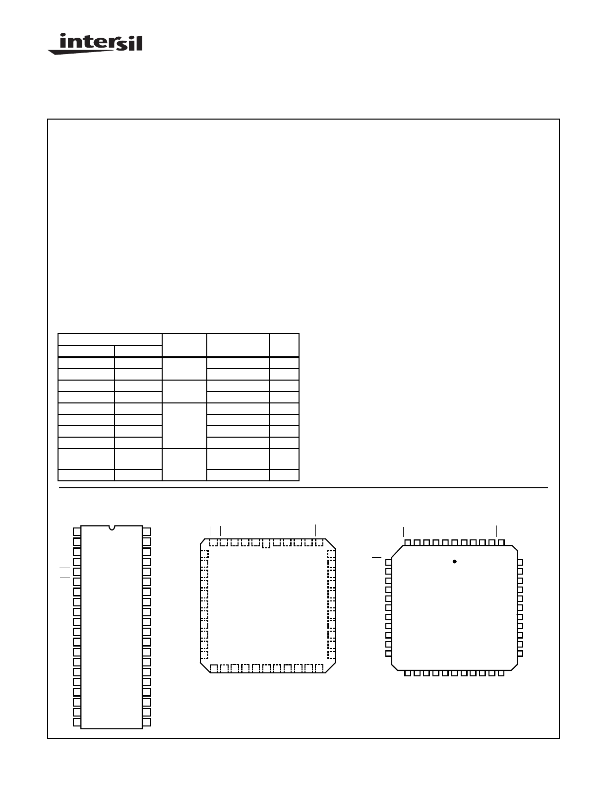
Pinouts
82C55A (DIP)
TOP VIEW
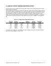
82C55A (CLCC)
TOP VIEW
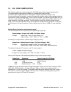
82C55A (PLCC)
TOP VIEW
PA3
PA2
PA1
PA0
RD
CS
GND
A1
A0
PC7
PC6
PC5
PC4
PC0
PC1
PC2
PC3
PB0
PB1
PB2
PA4
PA5
PA6
PA7
WR
RESE
T
D0
D1
D2
D3
D4
D5
D6
D7
V
CC
PB7
PB6
PB5
PB4
PB3
13
1
2
3
4
5
6
7
8
9
10
11
12
14
15
16
17
18
19
20
28
40
39
38
37
36
35
34
33
32
31
30
29
27
26
25
24
23
22
21
4065 321444342414
9
10
11
8
7
12
13
17
16
15
14
39
38
37
36
35
34
33
32
31
30
29
18 19 20 21 22 23 24 25 26 27 28
GND
NC
A1
A0
PC7
PC6
PC5
PC4
PC0
PC1
PC2
PC3
PB0
PB1
PB2
PB3
PB4
PB5
PB6
PB7
V
CC
NC
NC
RESET
D0
D1
D2
D3
D4
D5
D6
D7
NC
CS
RD
PA0
PA1
PA2
PA3
PA4
PA5
PA6
PA7
WR
CS
GND
A1
A0
PC7
PC6
PC5
PC4
PC0
PC1
PC3
PB0
PB1
PB2
PB3
PB4
PB5
PB6
PB7
NC
NC
RESET
D0
D1
D2
D3
D4
D5
D6
D7
V
CC
RD
PA0
PA1
PA2
PA3
PA4
PA5
PA6
PA7
WR
NC
PC2
NC
44 4342 4140
39
38
37
36
35
34
33
32
31
30
29
2827
123456
262524232221201918
7
8
9
10
11
12
13
14
15
16
17
File Number 2969.2
CAUTION: These devices are sensitive to electrostatic discharge; follow proper IC Handling Procedures.
http://www.intersil.com or 407-727-9207
| Copyright © Intersil Corporation 1999