


2
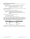
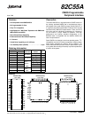
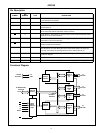
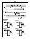
Functional Diagram
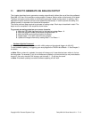
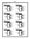
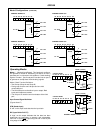
Pin Description
SYMBOL
PIN
NUMBER TYPE DESCRIPTION
V
CC
26 V
CC
: The +5V power supply pin. A 0.1µF capacitor between pins 26 and 7 is
recommended for decoupling.
GND 7 GROUND
D0-D7 27-34 I/O DATA BUS: The Data Bus lines are bidirectional three-state pins connected to the
system data bus.
RESET 35 I RESET: A high on this input clears the control register and all ports (A, B, C) are set
to the input mode with the “Bus Hold” circuitry turned on.
CS 6 I CHIP SELECT: Chipselect isanactive lowinput usedto enablethe 82C55Aonto the
Data Bus for CPU communications.
RD 5 I READ: Read is an active low input control signal used by the CPU to read status
information or data via the data bus.
WR 36 I WRITE: Write is an active low input control signal used by the CPU to load control
words and data into the 82C55A.
A0-A1 8, 9 I ADDRESS: These input signals, in conjunction with the RD and WR inputs, control
the selection of one of the three ports or the control word register. A0 and A1 are
normally connected to the least significant bits of the Address Bus A0, A1.
PA0-PA7 1-4, 37-40 I/O PORT A: 8-bitinput andoutput port. Bothbus holdhigh andbus holdlow circuitry are
present on this port.
PB0-PB7 18-25 I/O PORT B: 8-bit input and output port. Bus hold high circuitry is present on this port.
PC0-PC7 10-17 I/O PORT C: 8-bit input and output port. Bus hold circuitry is present on this port.
GROUP A
PORT A
(8)
GROUP A
PORT C
UPPER
(4)
GROUP B
PORT C
LOWER
(4)
GROUP B
PORT B
(8)
GROUP B
CONTROL
GROUP A
CONTROL
DATA BUS
BUFFER
READ
WRITE
CONTROL
LOGIC
RD
WR
A1
A0
RESET
CS
D7-D0
POWER
SUPPLIES
+5V
GND
BI-DIRECTIONAL
DATA BUS
I/O
PA7-PA0
I/O
PC7-PC4
I/O
PC3-PC0
I/O
PB7-PB0
8-BIT
INTERNAL
DATA BUS
82C55A