


EM78P458/459
OTP ROM
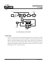
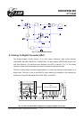
Fig. 11 Interrupt Input Circuit
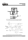
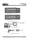
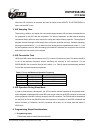
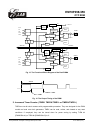
4.7 Analog-To-Digital Converter (ADC)
The analog-to-digital circuitry consists of an 8-bit analog multiplexer, three control registers
(ADCON/R9, AD-CMP-CON/IOCA0, GCON/IOC90), one data register (ADDATA/RA) and an ADC
with 8-bit resolution. The functional block diagram of the ADC is shown in Fig. 12. The analog
reference voltage (Vref) and analog ground are connected via separate input pins.
The ADC module utilizes successive approximation to convert the unknown analog signal into a
digital value. The result is fed to the ADDATA. Input channels are selected by the analog input
multiplexer via the ADCON register Bits ADIS0, ADIS1, and ADIS2.
01234567
OP2
GCON
543 210
ADDATA
OP1
DATA BUS
ADC4
ADC3
ADC2
ADC1
ADC5
ADC6
ADC7
ADC8 Vref
Power-Down
Fsco
Internal
RC
4-1
MUX
234 34
ADC
( successive approximation )
3
8-1 Analog Switch
01012
AD-CMPCON RFAD-CMPCON ADCON ADCON
+
+
-
-
Start to Convert
This specification is subject to change without prior notice. 07.01.2003 (V1.3)
31
Fig. 12 The Functional Block Diagram of Analog-to-Digital Conversion