2 IMPLEMENTING THE DEBUG MONITOR
EPSON S1C33 FAMILY DEBUG MONITOR
OPERATION MANUAL
4
2 Implementing the Debug Monitor
This chapter describes how to implement the debug monitor and how to start it from the application
program.
2.1 Resources Required for the Debug Monitor
The debug monitor uses the following resources:
• Approximately 10KB of ROM area for the program code of the debug monitor.
• Approximately 2.5KB of RAM area for the work and stack area.
• Since the debug monitor uses the debugging exception of the CPU, addresses 0x0 to 0xF of the built-in RAM area
are used as the vector and stack for processing debugging exceptions. Furthermore, addresses 0x10 to 0x2F are
reserved for extending functions.
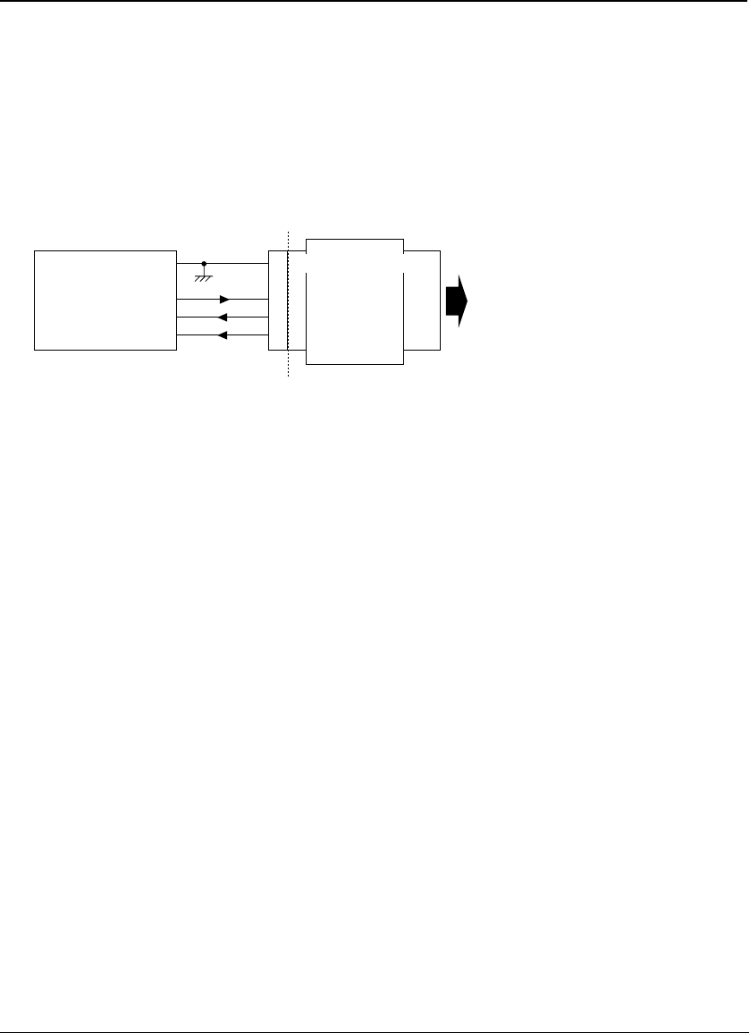
• One channel (Ch.0 or Ch.1) of the serial interface (8-bit asynchronous mode) is used for communicating with the
debugger db33 on the personal computer.
Figure 2.1.1 shows a connection diagram.
VSS
SOUT0/1
SIN0/1
SCLK0/1
Connected to the personal computer
using the RS232C cable
(Baud rate: 115,200 bps)
S1C33xxx
Target board
S5U1C330MxD1
Figure 2.1.1 RS232C connector diagram
• Communication via RS232C is performed by a software polling method without any interrupt related resource.
• A serial I/O device outside the S1C33 chip can be used by customizing the serial I/O routine (see Section 2.4).
• S5U1C330M2S uses the TXD, RXD and status registers of the corresponding serial interface channel exclusively.
Therefore, do not access these control registers.
Furthermore, fix the I/O pins for the channel at the serial interface pins using the port function select register. For
example, the sample program "m3s_sci.s" writes 0x07 to the P0 function select register (0x402D0) when Ch.0 is
used or 0x70 when Ch.1 is used to set the serial interface pins.


