APPENDIX S5U1C330MXD1 BOARD
S1C33 FAMILY DEBUG MONITOR EPSON
OPERATION MANUAL
15
Appendix S5U1C330MxD1 Board
This chapter describes how to use the S5U1C330MxD1 board.
A.1 Outline of S5U1C330MxD1 Board
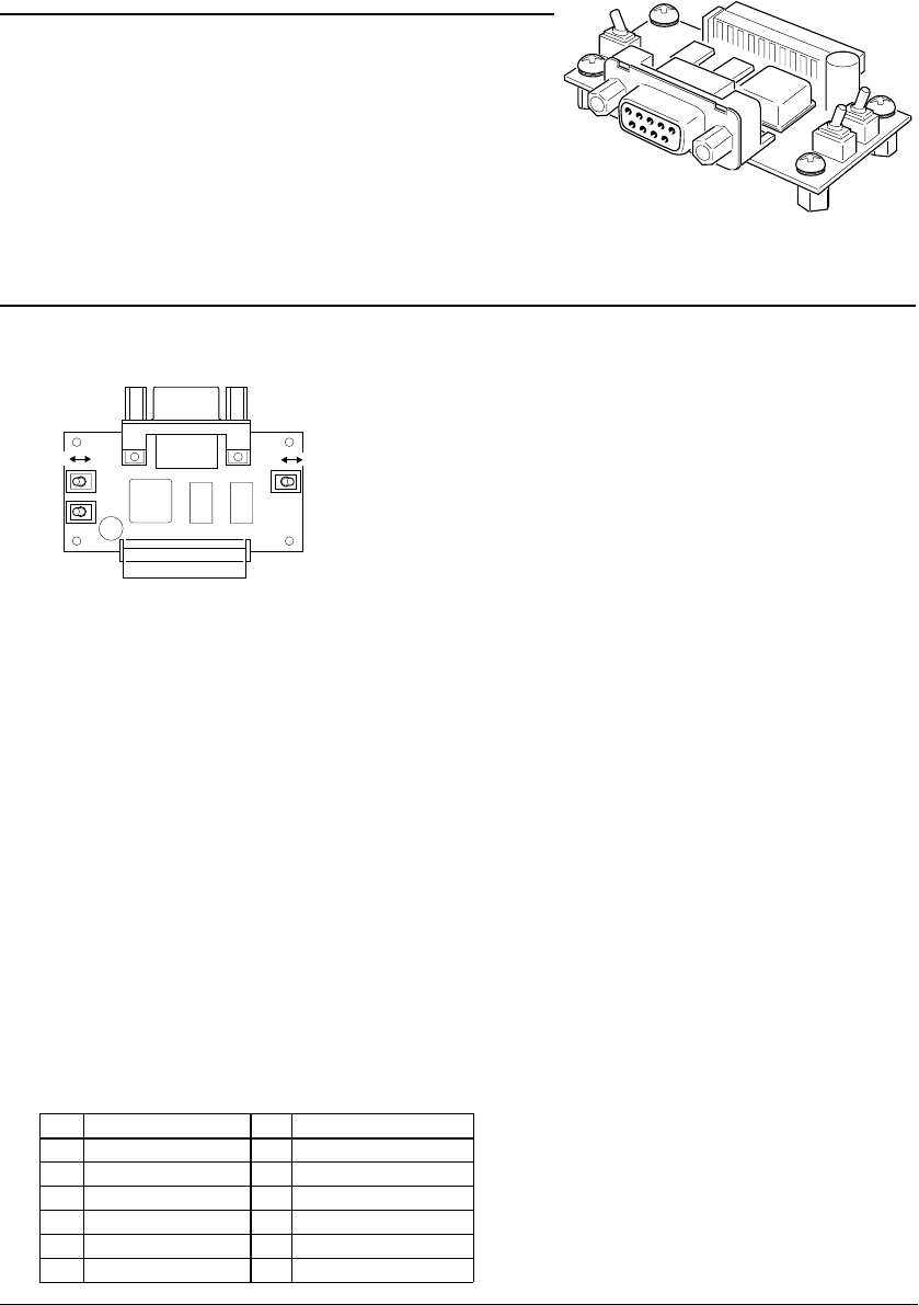
The S5U1C330MxD1 board provides the interface for the debug
monitor to the demonstration tools such as the S5U1C33104Dx or the
user target board. The S5U1C330MxD1 allows on-board debugging
using the debugger (db33.exe) on a personal computer by connecting
it to the target board in which the S1C33 Family debug monitor
(S5U1C330M2S) has been implemented.
Two types of boards are available: S5U1C330M1D1 board for 5 V
operation and S5U1C330M2D1 for 3.3 V operation.
Figure A.1.1 S5U1C330MxD1 board
A.2 Names and Functions of Each Part
The following describes the parts layout on the S5U1C330MxD1 board as well as the functions of the connectors and
switches:
RS232 connector
SW1
(RESET)
SW2
(NMI)
SW3
(DEBUG)
S5U1C33xxxDx/target board I/F connector
ONOFF
112
ONOFF
Figure A.2.1 S5U1C330MxD1 board layout
SW1 (RESET switch)
Sets up the status of the RESET pin at the S5U1C33xxxDx/
target board I/F connector. When a S5U1C33xxxDx board is
connected, this switch can reset the CPU on the board.
ON: RESET = "0" OFF: RESET = "1"
SW2 (NMI switch)
Sets up the status of the NMI pin at the S5U1C33xxxDx/target
board I/F connector. When a S5U1C33xxxDx board is
connected, a NMI request can be input to the CPU on the
board.
ON: NMI = "0" OFF: NMI = "1"
SW3 (DEBUG switch)
Sets up the status of the DEBUG pin at the S5U1C33xxxDx/target board I/F connector. When the
S5U1C33104Dx/S5U1C33209Dx board is connected, the switch signal is input to the K63 port and can be used
to start up the debug monitor from the boot routine.
ON: DEBUG (K63) = "0" OFF: DEBUG (K63) = "1"
When the switch is ON, the S5U1C33104Dx/S5U1C33209Dx will start the debug monitor. When the switch is
OFF, the S5U1C33104Dx/S5U1C33209Dx will start executing the program stored in the Flash memory. The
S5U1C33104Dx/S5U1C33209Dx works assuming the debug switch is OFF when the S5U1C330MxD1 is not
connected.
RS232C connector
This is a Dsub 9-pin connector for connecting a personal computer. Use the RS232C cable supplied with the
S5U1C330MxD1 package for connection.
S5U1C33xxxDx/target board I/F connector
This connector is used for connecting the S5U1C33xxxDx board. The pin layout is as follows:
Table A.2.1 S5U1C33xxxDx/target board connector pin layout
No. Signal name No. Signal name ( ) indicates the CPU pin corresponding to the signal
1VCC [+5 V, +3.3 V] 7 N.C. when the S5U1C33104Dx/S5U1C33209Dx is
2VCC [+5 V, +3.3 V] 8 DEBUG (K63) connected.
3 RESET (#RESET) 9 VCC [+5 V, +3.3 V] Since the corresponding signals on the
4 TxD (P05) 10 SCLK (P06) S5U1C33xxxDx may differ depending on the
5 RxD (P04) 11 GND board, refer to the pin layout table provided in
6 NMI (#NMI) 12 GND the specifications of each S5U1C33xxxDx board.


