


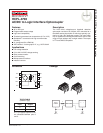

HCPL-3700 AC/DC to Logic Interface Optocoupler
©2005 Fairchild Semiconductor Corporation www.fairchildsemi.com
HCPL-3700 Rev. 1.0.1 4
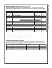
Switching Characteristics (T
A
= 25°C, V
CC
= 5 V Unless otherwise specified)
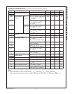
Package Characteristics
(T
A
= 0°C to 70°C Unless otherwise specified)
Notes:
6. T
PHL
propagation delay is measured from the 2.5V level of the leading edge of a 5.0V input pulse (1µs rise time) to
the 1.5 V level on the leading edge of the output pulse. T
PLH
propagation delay is measured on the trailing edges
of the input and output pulse. (Refer to Fig. 9)
7. Common mode transient immunity in logic high level is the maximum tolerable (positive) dV
cm
/dt on the leading
edge of the common mode pulse signal V
CM
, to assure that the output will remain in a logic high state (i.e., V
O
>
2.0 V). Common mode transient immunity in logic low level is the maximum tolerable (negative) dV
cm
/dt on the
trailing edge of the common mode pulse signal, V
CM
, to assure that the output will remain in a logic low state
(i.e., V
O
< 0.8 V). Refer to Fig. 10.
8. In applications where dV
cm
/dt may exceed 50,000 V/µs (Such as static discharge), a series resistor, R
CC
,
should be included to protect the detector chip from destructive surge currents. The recommended value for
R
CC
is 240V per volt of allowable drop in V
CC
(between pin 8 and V
CC
) with a minimum value of 240Ω.
9. Device is considered a two terminal device: Pins 1, 2, 3 and 4 are shorted together and Pins 5, 6, 7 and 8 are
shorted together.
10. The 2500 V
RMS
/1 min. capability is validated by a 3.0 kV
RMS
/1 sec. dielectric voltage withstand test.
11. AC voltage is instantaneous voltage for V
TH+
& V
TH-
.
12. All typicals at T
A
= 25°C, V
CC
= 5V unless otherwise specified.
Symbol AC Characteristics Test Conditions Min. Typ. Max. Unit
T
PHL
Propagation Delay Time
(to Output Low Level)
R
L
= 4.7kΩ, C
L
= 30pF
(6)
6.0 15 µs
T
PLH
Propagation Delay Time
(to Output High Level)
R
L
= 4.7kΩ, C
L
= 30pF
(6)
25.0 40 µs
t
r
Output Rise Time (10–90%) R
L
= 4.7kΩ, C
L
= 30pF 45 µs
t
f
Output Fall Time (90–10%) R
L
= 4.7kΩ, C
L
= 30pF 0.5 µs
|CM
H
| Common Mode Transient
Immunity (at Output High Level)
I
IN
= 0 mA, R
L
= 4.7kΩ,
V
O min
= 2.0 V, V
CM
= 1400V
(7)(8)
4000 V/µs
|CM
L
| Common Mode Transient
Immunity (at Output Low Level)
I
N
= 3.11mA, R
L
= 4.7kΩ,
V
O max
= 0.8V, V
CM
= 140V
(7)(8)
600 V/µs
Symbol Characteristics Test Conditions Min. Typ. Max. Unit
V
ISO
Withstand Insulation Voltage Relative humidity < 50%,
T
A
= 25°C, t = 1 min,
I
I-O
≤ 2µA
(9)(10)
2500 V
RMS
R
I-O
Resistance (input to output) V
IO
= 500Vdc
(9)
10
12
Ω
C
I-O
Capacitance (input to output) f = 1MHz, V
IO
= 0Vdc 0.6 pF