Change even page title here
Chapter 5 Configuration of the Evaluation-Board
UG-900001-32 - 12 - © Fujitsu Microelectronics Europe GmbH
5.1 Modifications for use with MB90470 / MB90480 series
Some modifications have to be done in order to use the FLASH-CAN-100P Board together
with a MCU of the MB90470 / MB90480 series:
1. Check that U6 is MAX3232CPE
2. Change R6 470 => 390 Ohm. Check that output voltage of U3 is 3.3V (JP2)
3. Disassemble C10 (100nF)
4. Connect J4- Pin 27 to JP10- Pin 2 (SIN)
5. Connect J4- Pin 28 to JP9- Pin 2 (SOT)
6. Connect J5- Pin 80 to GND (X0A) if no Sub-Clock is used
Otherwise Sub-Clock crystal Y2 and capacitors C5, C6 has to be assembled
7. Remove JP1. Connect JP1- Pin 2 to JP2- Pin 1
8. Emulator-Settings:
Only MB90470series:
The MB90470 series normally uses 3V power-supply. However, some Ports (P2, P3, P4 and
P7) can operate with 5V. In this case Pin 23 (Vcc5) of the microcontroller has to be
disconnected from Vcc on the FLASH-CAN-100P Board but has to be connected to +5V.
Cutting a trace near the capacitor CB2 on the bottom layer of the board only can do this.
Caution with the probe-cable:
The probe-cable MB2132-457 (Yamaichi socket) can NOT be used for dual voltage
(Vcc3=+3V, Vcc5=+5V), because Pin 23 and Pin 84 (Vcc3 / Vcc5) are shortcut within the
probe-cable.
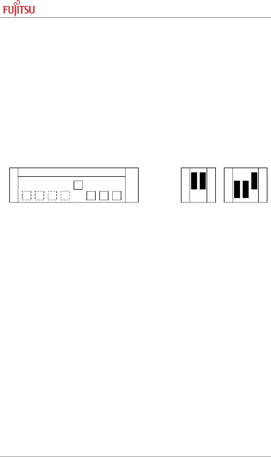
S1
A B C
S2
A B C
ON
OFF
SW1
1 2 3 4 5 6 7 8
check emulator-manual for clock-selection-switch


