


5K320 SATA OEM Specification
113
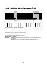
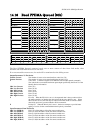
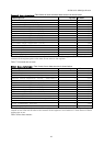
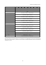
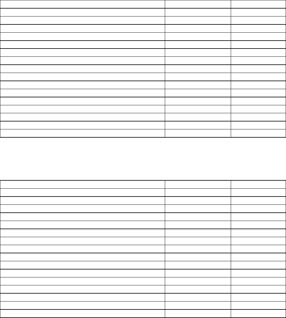
Command data structure: Data format of each command data structure is shown below.
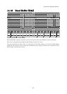
Description Bytes Offset
Device Control register 1 00h
Features register (7:0) (see Note) 1 01h
Features register (15:8) 1 02h
Sector count register (7:0) 1 03h
Sector count register (15:8) 1 04h
Sector number register (7:0) 1 05h
Sector number register (15:8) 1 06h
Cylinder Low register (7:0) 1 07h
Cylinder Low register (15:8) 1 08h
Cylinder High register (7:0) 1 09h
Cylinder High register (15:8) 1 0Ah
Device register 1 0Bh
Command register 1 0Ch
Reserved 1 0Dh
Timestamp (milliseconds from Power-on) 4 0Eh
18
Note: bits (7:0) refer to the most recently written contents of the register. Bits (15:8) refer to the
contents of the register prior to the most recent write to the register.
Table 77 Command data structure
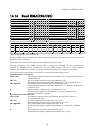
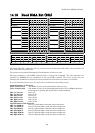
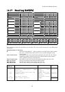
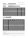
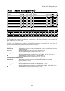
Error data structure: Data format of error data structure is shown below.
Description Bytes Offset
Reserved 1 00h
Error register 1 01h
Sector count register (7:0) (see Note) 1 02h
Sector count register (15:8) (see Note) 1 03h
Sector number register (7:0) 1 04h
Sector number register (15:8) 1 05h
Cylinder Low register (7:0) 1 06h
Cylinder Low register (15:8) 1 07h
Cylinder High register (7:0) 1 08h
Cylinder High register (15:8) 1 09h
Device register 1 0Ah
Status register 1 0Bh
Extended error data (vendor specific) 19 0Ch
State 1 1Fh
Life timestamp (hours) 2 20h
34
Note: bits (7:0) refer to the contents if the register is read with bit 7 of the Device Control register
cleared to zero. Bits (15:8) refer to the contents if the register is read with bit 7 of the Device Control
register set to one.
Table 78 Error data structure