


Page 5 of 8 Version 1.0 11/08/01
plane. In most circumstances, however, it is prudent to place a filter circuit on AVDD;
refer to the CPC710 DD3.x User’s Manual for more information.
Ø The PLL is now set up and controlled by external signals PLL_RANGE [1:0] and 6
external signals PLL_TUNE [5:0] instead of PLL133 and PLL_TUNE [1:0]. This is a
change from the previous revision.
Packaging Changes:
v FC-PBGA Package instead of CBGA
Ø The CPC710 DD3.x is offered in a 35mm 728 pin FC-PBGA (Flip Chip Plastic Ball Grid
Array) package. This is a change from the previous revision – the DD3.x is not
pin/package compatible with the DD2. Refer to the CPC710-133 PCI Bridge and Memory
Controller Datasheet for more details on the physical packaging.
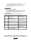
v I/O Pinout Deletions:
The following I/Os are no longer present on the DD3 revision:
INTERFACE SIGNAL NAME IMPACT
Memory
Interface
SDCS_12, SDCS_13, SDCS_14,
SDCS_15
SDRAS_2, SDRAS_3
SDCAS_2, SDCAS_3
WE_2, WE_3
Changes to the memory interface.
Refer to Chapter 6 Of User’s
Manual for more details.
PCI 32-bit
Interface
P_GNT_6, P_GNT_5, P_GNT_4,
P_REQ_6, P_REQ_5, P_REQ_4
Decreases number of PCI devices
supported by the internal bus
arbiter, unless multiplexed (see
below).
PCI 32-bit
Interface
P_ISA_MASTER
PCI 32-bit
Interface
P_CFG [0:2] CFGA [13:11] no longer driven
offchip (used for save loads on PCI
bus)
PCI 64-bit
Interface
G_CFG [0:2] CFGA [13:11] no longer driven
offchip
Clock Inputs PLL_133, PLN_RTC_CLOCK DD3 has new strapping options.
Timers now controlled only by
PCI32 clock.
Test Signals CE1_A, CE1_B, CE1_C1, CE1_C2, DI1,
DI2, CE0_IO, RI, SCAN_GATE,
TESTIN, CE_TRST, TESTOUT
Signals used only by manufacturing
test.