


Page 6 of 8 Version 1.0 11/08/01
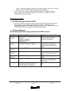
v I/O Pin Additions:
The following I/Os are new on the DD3 revision:
INTERFACE SIGNAL NAME IMPACT
60x bus Interface SYS_BG2_, SYS_BG3_, SYS_MCP2,
SYS_MCP3, SYS_HRESET2,
SYS_HRESET3, SYS_SRESET2,
SYS_SRESET3
New for 4-way CPU support
60x bus Interface
SYS_TA_HIT
Memory Interface MADDR13 Used for newer memory sizes
Clock Inputs PLL_RANGE0, PLL_RANGE1,
PLL_TUNE2, PLL_TUNE3, PLL_TUNE4,
PLL_TUNE5
New; used for setup and control
of PLL
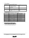
v I/O Pins Multiplexed:
The following I/Os are multiplexed on the DD3 revision:
INTERFACE PIN FUNCTION OPTION REGISTER BIT TO USE
TO SELECT FUNCTION
Memory Interface SDRAS_1 becomes SDQM SDRAM0_MCCR [14] = 1
Memory Interface SDCAS_1 becomes SDQM SDRAM0_MCCR [14] = 1
Memory Interface WE_1 becomes SDQM SDRAM0_MCCR [14] = 1
Memory Interface G_ARB becomes SDQM SDRAM0_MCCR [15] = 1
60x bus Interface DRAMREQ_ becomes NODLK_ CPC0_PGCHP [20] = 0
60x bus Interface DRAMGNT_ becomes DLK_ CPC0_PGCHP [20] = 0
PCI 64-bit Interface G_REQ_7 becomes P_REQ_6 CPC0_PGCHP [23] = 1
PCI 64-bit Interface G_GNT_7 becomes P_GNT_6 CPC0_PGCHP [23] = 1
PCI 64-bit Interface G_REQ_6 becomes P_REQ_5 CPC0_PGCHP [22] = 1
PCI 64-bit Interface G_GNT_6 becomes P_GNT_5 CPC0_PGCHP [22] = 1
PCI 64-bit Interface G_REQ_5 becomes P_REQ_4 CPC0_PGCHP [21] = 1
PCI 64-bit Interface G_GNT_5 becomes P_GNT_4 CPC0_PGCHP [21] = 1
Hardware ID Changes for DD3.0 revision:
v PCI-32 revision ID in PCIC0_REVID = x’03
v PCI-64 revision ID in PCIC1_REVID = x’03
v EC Level in CPC0_UCTL [24:31] = x’a0